SDRlab 122-16 External Clock
Overview
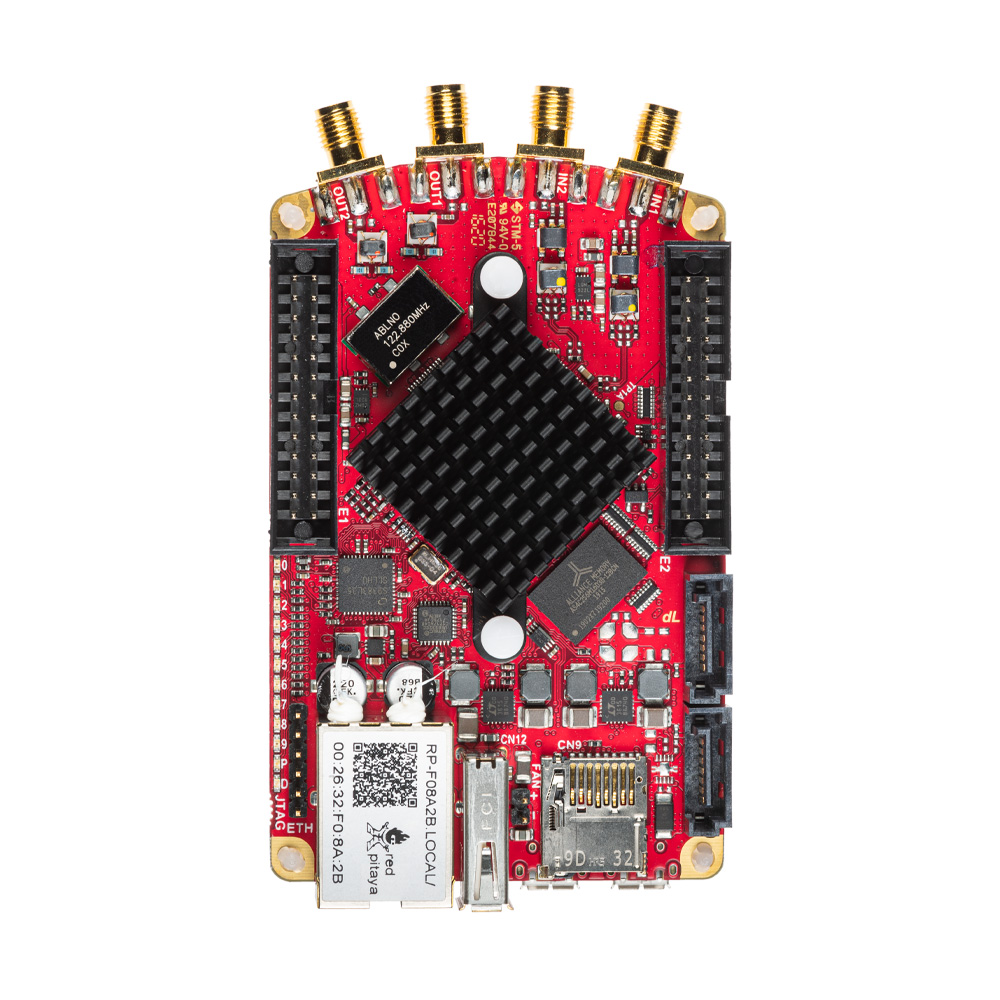
The SDRlab 122-16 External Clock is a modified version of the standard SDRlab 122-16 that has been hardware-modified to accept an external clock source. This variant is optimized for SDR applications requiring clock synchronisation with external equipment.
Features
16-bit ADC and 14-bit DAC, 122.88 MS/s (at 122.88 MHz clock)
AC-coupled 50 Ω RF inputs and outputs
SDR-optimized clock frequency (122.88 MHz)
External clock input support (pre-modified hardware)
Dual-core ARM Cortex-A9 processor
FPGA Xilinx Zynq 7020 SoC
512 MB RAM
22 digital I/Os, 4 analog inputs, 4 analog outputs
Multiple communication interfaces: I2C, SPI, UART, CAN
Micro USB connectivity for power and console
Quick Reference
Category |
Key Specifications |
|---|---|
ADC |
2 channels, 16-bit, 122.88 MS/s |
DAC |
2 channels, 14-bit, 122.88 MS/s |
Processor |
Dual-core ARM Cortex-A9 |
FPGA |
Xilinx Zynq 7020 SoC |
RAM |
512 MB |
Digital I/O |
22 GPIOs @ 3.3V |
Analog I/O |
4 inputs (12-bit), 4 outputs (8-bit) |
Connectivity |
Ethernet, USB-C, Extension connectors |
Input Impedance |
50 Ω (AC-coupled) |
Special Features |
AC-coupling, External clock input (LVDS) |
Differences from Standard SDRlab 122-16
This board is electrically identical to the SDRlab 122-16 with the following hardware changes already applied at the factory:
Parameter |
SDRlab 122-16 |
SDRlab 122-16 External Clock |
|---|---|---|
On-board 122.88 MHz oscillator |
Active (drives ADC, FPGA, DAC) |
Bypassed (disconnected from clock path) |
E2 pins 23-24 (Ext. ADC Clk±) |
Not connected |
Active — must receive a valid LVDS clock |
External ADC clock |
No (requires hardware modification) |
Yes (pre-modified, plug-and-use) |
Operation without external clock |
Normal (uses onboard oscillator) |
FPGA non-functional; PS boots from 33 MHz |
Warning
The onboard oscillator is bypassed. The board will not perform signal acquisition or generation without a valid external LVDS clock on E2 pins 23-24. Supplying the wrong signal level or leaving the pins floating will prevent FPGA operation.
Note
When using this board with synchronisation features:
X-channel 2.0 (Click Shield) synchronisation is compatible with this board.
X-channel synchronisation is not compatible.
Technical Specifications
The SDRlab 122-16 External Clock has the same specifications as the standard SDRlab 122-16, with the following addition:
External ADC clock: Yes (hardware pre-modified for external clock input)
Hardware modification: Resistors relocated to enable external clock input
For full technical specifications, please refer to the SDRlab 122-16 specifications.
See also
For more detailed information, please refer to the Original Gen board comparison table.
Performance & Measurements
Note
We do not have explicit measurements for the SDRlab 122-16 board.
You can find the measurements of the fast analog frontend for similar boards here:
Schematics & 3D Models
Schematics
Note
The external clock variant uses the same PCB as the standard SDRlab 122-16. The only physical difference is the relocation of resistors R25, R26 to R23, R24.
Mechanical Specifications & 3D Models
Advanced Features
External ADC Clock
The main ADC, DAC, and FPGA CLK signal can be supplied from an external source through the Ext. ADC Clk± ports on the E2 connector connector.
Signal Path
The clock signal travels directly through the ADC, then to the FPGA, and DAC, ensuring consistent timing across the signal acquisition path.
External Clock Specifications
The external clock should be a differential LVDS signal:
Parameter |
Description |
Min |
Typ |
Max |
Unit |
|
|---|---|---|---|---|---|---|
Clock input pins |
23 (Clk+) and 24 (Clk-) on E2 connector |
|||||
Input standards |
LVDS |
|||||
Input clock coupling |
AC (on-board capacitors) |
|||||
\(f_{CLK}\) |
Input frequency range |
ADC and DAC dependant |
1 |
125 |
MHz |
|
\(V_{ID,DIFF,PP}\) |
Input voltage swing |
Differential peak-to-peak |
0.35 |
0.8 |
V |
|
IDC |
Input clock duty cycle |
45% |
55% |
|||
Note
The typical operating frequency depends on the board variant:
STEMlab 125-14: 125 MHz
SDRlab 122-16: 122.88 MHz
Operating outside the board’s specified frequency is possible but voids all performance guarantees. See the warning below.
For exact voltage levels and timing requirements, please refer to the oscillator datasheet.
Warning
Not a reference clock input: The Ext. ADC Clk± ports are not a reference clock input for a PLL or any other timing circuit. They directly drive the main sampling clock for the ADC, DAC, and FPGA. Connecting a reference clock signal intended for a PLL will not function as expected.
Warning
Changing the external clock frequency during operation is not supported.
The Zynq 7010/7020 PL uses Mixed-Mode Clock Managers (MMCMs) and PLLs to derive internal fabric clocks from the input clock. Changing the external clock frequency during operation will cause the MMCM/PLL to lose lock, resulting in undefined output clocks and acquisition/generation errors. A full FPGA reset or reconfiguration is required after any clock frequency change.
Note
Operating at non-standard clock frequencies:
The Red Pitaya FPGA is designed, tested, and guaranteed to operate correctly at the board’s specified core clock frequency (125 MHz for STEMlab 125-14, 122.88 MHz for SDRlab 122-16, etc).
While it is possible to run the board at different clock frequencies, please be aware that:
FPGA functionality: The official FPGA configuration may not function as intended at non-standard frequencies and requires thorough testing
Sampling rates: The ADC and DAC sampling rates will change proportionally with the clock frequency
Analog bandwidth: The analog bandwidth of the board will change with the clock frequency
Absence of external clock:
OS 2.07-48 or higher: If no valid external clock is present, the PS side will boot using an internal 33 MHz oscillator, but the FPGA will not operate (no signal acquisition/generation functionality)
OS versions prior to 2.07-48: The board will fail to boot (stuck in reboot cycle) if no valid external clock is detected
Note
Advanced: Dynamic clock reconfiguration
The standard Red Pitaya FPGA bitstream does not implement the Dynamic Reconfiguration Port (DRP) interface that AMD (Xilinx) provides for runtime MMCM/PLL reconfiguration. A custom FPGA design using DRP-based MMCM reconfiguration with active lock monitoring could theoretically support runtime clock frequency changes, but this requires extensive FPGA development and verification. The PS side (ARM/Linux) is not affected by clock changes, as it runs from its own independent 33 MHz crystal-derived PLL.
Additional Resources
For additional specifications, please refer to:
SDRlab 122-16 - Standard SDRlab 122-16 specifications
Original Gen hardware specifications - Common Original Gen specifications
Original Gen board comparison table - Comparison across all Red Pitaya Original Gen models
Legal & Disclaimers
Note
The information provided by Red Pitaya d.o.o. is believed to be accurate and reliable. However, no liability is accepted for its use. Please note that the contents may be subject to change without prior notice.