SDRlab 122-16
Overview
The SDRlab 122-16 is a specialized Red Pitaya board designed for Software Defined Radio (SDR) applications. It features 16-bit ADC and 14-bit DAC resolution with 122.88 MS/s sampling rate, optimized for RF signal processing. The board includes AC-coupled 50 Ω inputs and operates at the SDR-standard 122.88 MHz clock frequency.
Features
16-bit ADC and 14-bit DAC, 122.88 MS/s
AC-coupled 50 Ω RF inputs and outputs
SDR-optimized clock frequency (122.88 MHz)
Dual-core ARM Cortex-A9 processor
FPGA Xilinx Zynq 7020 SoC
512 MB RAM
22 digital I/Os, 4 analog inputs, 4 analog outputs
Multiple communication interfaces: I2C, SPI, UART, CAN
Micro USB connectivity for power and console
Quick Reference
Category |
Key Specifications |
|---|---|
ADC |
2 channels, 16-bit, 122.88 MS/s |
DAC |
2 channels, 14-bit, 122.88 MS/s |
Processor |
Dual-core ARM Cortex-A9 |
FPGA |
Xilinx Zynq 7020 SoC |
RAM |
512 MB |
Digital I/O |
22 GPIOs @ 3.3V |
Analog I/O |
4 inputs (12-bit), 4 outputs (8-bit) |
Connectivity |
Ethernet, USB-C, Extension connectors |
Input Impedance |
50 Ω (AC-coupled) |
Special Features |
AC-coupling, 16-bit resolution |
Board Layout & Pinout
Technical Specifications
Parameter |
Value |
Units |
Notes |
|---|---|---|---|
|
|||
Processor |
Dual core ARM Cortex-A9 |
- |
|
FPGA |
FPGA AMD (Xilinx) Zynq 7020 SoC |
- |
|
RAM |
512 |
MB |
(4 Gb) |
Core clock frequency |
122.88 |
MHz |
|
System memory |
Micro SD up to 32 GB |
- |
|
Serial console connector |
Micro USB |
- |
|
Power connector |
Micro USB |
- |
|
Power consumption |
5 V, 2 A |
- |
max |
|
|||
Ethernet |
1 |
Gbit |
|
USB |
USB-A 2.0 |
- |
|
Wi-Fi |
Requires Wi-Fi dongle |
- |
|
|
|||
RF input channels |
2 |
- |
|
Sampling rate |
122.88 |
MS/s |
|
ADC resolution |
16 |
bit |
|
Input impedance |
50 Ω |
- |
|
Full scale voltage range |
0.5 Vpp / -2 dBm |
- |
|
Input coupling |
AC |
- |
|
Absolute max. input voltage |
DC max 50 V (AC-coupled)
1 Vpp for RF
|
V |
|
Input ESD protection |
No |
- |
AC coupling [1] |
Overload protection |
DC voltage protection |
- |
|
Bandwidth |
300 kHz - 60 MHz |
- |
Undersampling up to 550 MHz |
Connector type |
SMA |
- |
|
|
|||
RF output channels |
2 |
- |
|
Sampling rate |
122.88 |
MS/s |
|
DAC resolution |
14 |
bit |
|
Load impedance |
50 Ω |
- |
|
Voltage range |
0.5 Vpp / -2 dBm |
- |
|
Output coupling |
AC |
- |
|
Short circuit protection |
No |
- |
AC coupling only |
Bandwidth |
300 kHz - 60 MHz |
- |
|
Connector type |
SMA |
- |
|
|
|||
Digital GPIOs |
22 |
- |
|
Digital voltage levels |
3.3 |
V |
|
Analog inputs |
4 |
- |
|
Analog input voltage range |
0 - 7.0 |
V |
|
Analog input resolution |
12 |
bit |
|
Analog input sampling rate |
100 |
kS/s |
|
Analog outputs |
4 |
- |
|
Analog output voltage range |
0 - 1.8 |
V |
|
Analog output resolution |
8 |
bit |
|
Analog output sampling rate |
≲ 3.2 |
MS/s |
|
Analog output bandwidth |
≈ 160 |
kHz |
|
Communication interfaces |
I2C, SPI, UART, CAN |
- |
|
Available voltages |
+5, +3.3 |
V |
|
External ADC clock |
No |
- |
See [2] |
|
|||
External trigger input |
DIO0_P |
- |
E1 connector |
External trigger input impedance |
Hi-Z |
- |
Digital input |
Trigger output |
DIO0_N |
- |
E1 connector [3] |
Daisy chain connectors (S1 & S2) |
Yes |
- |
|
Daisy chain connectors speed |
up to 500 |
Mb/s |
|
Daisy chain connectors type |
SATA |
- |
|
Ref. clock input |
N/A |
- |
|
Ref. clock frequency |
N/A |
- |
|
Ref. clock connector type |
N/A |
- |
|
|
|||
SD card |
Yes |
- |
|
QSPI |
Not populated |
- |
|
eMMC |
N/A |
- |
|
|
|||
Operating Temperature Range |
0 to 55 |
℃ |
With default heatsink |
Operating Humidity Range |
< 90% |
RH |
|
Automatic Shutdown Temperature |
85 |
℃ |
|
|
|||
Size (L x W x H) |
106.8 x 60.0 x 21.1 |
mm |
See Schematics for details |
Note
The SDRlab 122-16 operates at 122.88 MHz, which is a standard clock frequency for SDR applications.
Note
RF signal polarity
The SDRlab 122-16 analog front end introduces a 180 degree phase inversion on both RF inputs and RF outputs.
A sine burst applied to IN1 or IN2 is acquired as
-sine.A generated sine burst appears at the corresponding RF output as
-sine.
In analog loopback, the input and output inversions add up to 360 degrees, so this polarity change is usually not noticeable.
See also
For more detailed information, please refer to the Original Gen board comparison table.
Warning
Maximum Input Voltage
RF signal: 1 Vpp maximum (0.5 Vpp nominal)
DC voltage: up to 50 V (inputs are AC-coupled — DC will not pass to the ADC)
Exceeding the RF input level may damage the board permanently.
Performance & Measurements
Note
We do not have explicit measurements for the SDRlab 122-16 board.
You can find the measurements of the fast analog frontend for similar boards here:
Schematics & 3D Models
Schematics
Note
Full hardware schematics for the Red Pitaya board are not available. Red Pitaya has open-source code but not open hardware schematics. Nonetheless, development schematics are available. This schematic will give you information about hardware configuration, FPGA pin connections, and similar.
Mechanical Specifications & 3D Models
Hardware Details
Components
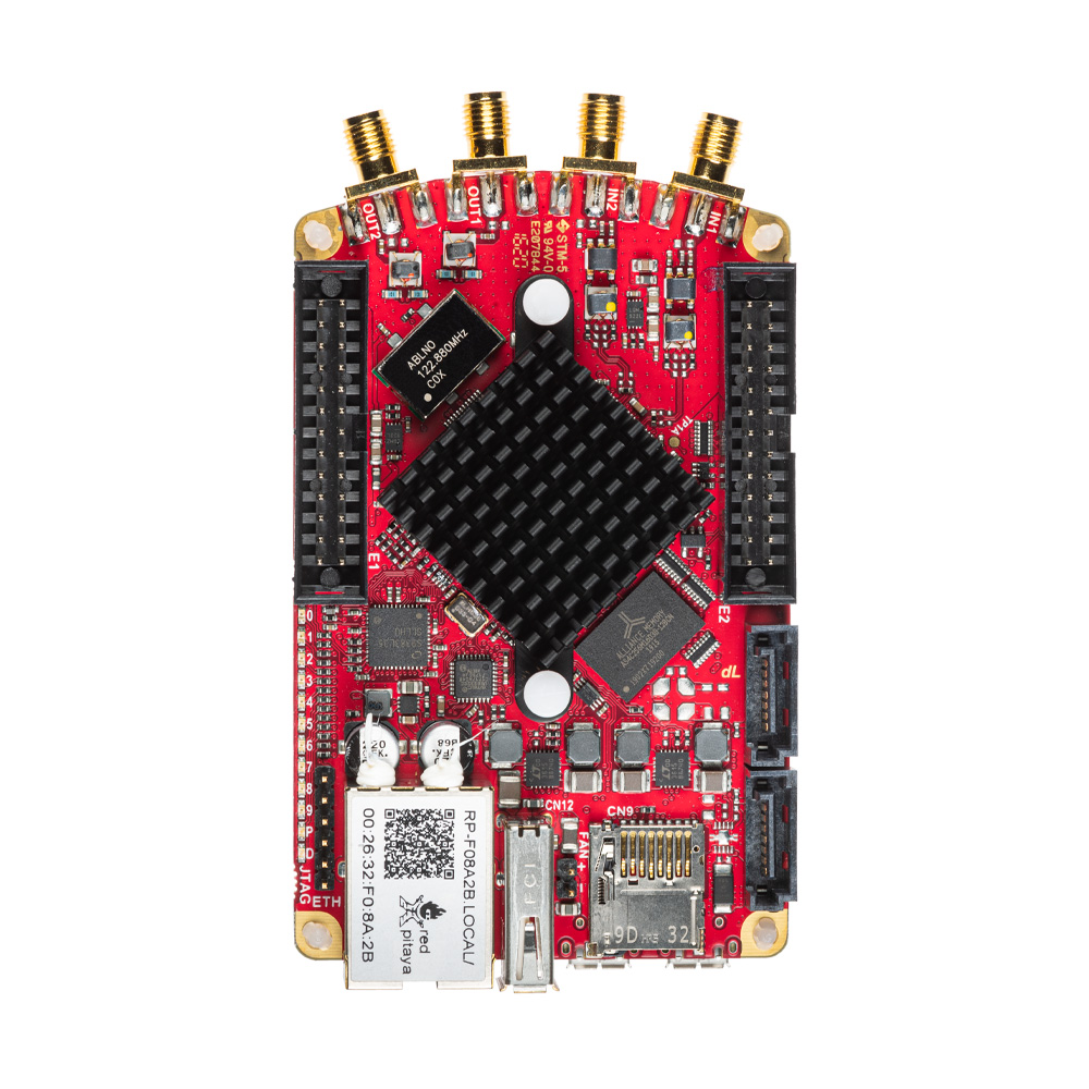
The SDRlab 122-16 uses high-performance analog components optimized for SDR (Software Defined Radio) applications.
ADC: Analog Devices LTC2185
Dual 16-bit, up to 250 MS/s ADC (operated at 122.88 MS/s)
Low noise, high dynamic range
AC-coupled inputs for RF applications
DAC: Analog Devices AD9767
Dual 14-bit, 125 MS/s DAC (operated at 122.88 MS/s)
High SFDR performance
Low power operation
FPGA: Xilinx Zynq 7020
Dual-core ARM Cortex-A9 @ 667 MHz
Larger programmable logic fabric than Zynq 7010
Integrated peripherals and memory controllers
Oscillator: ABRACON ABLNO 122.88 MHz
High-precision 122.88 MHz reference oscillator (SDR-standard frequency)
DC-DC Converter: LTC3615
High-efficiency step-down regulator
DDR3 SRAM: MT41J256M16HA-125
512 MB DDR3 RAM
QSPI Flash: S25FL128SAGNFI001
Not populated on standard boards
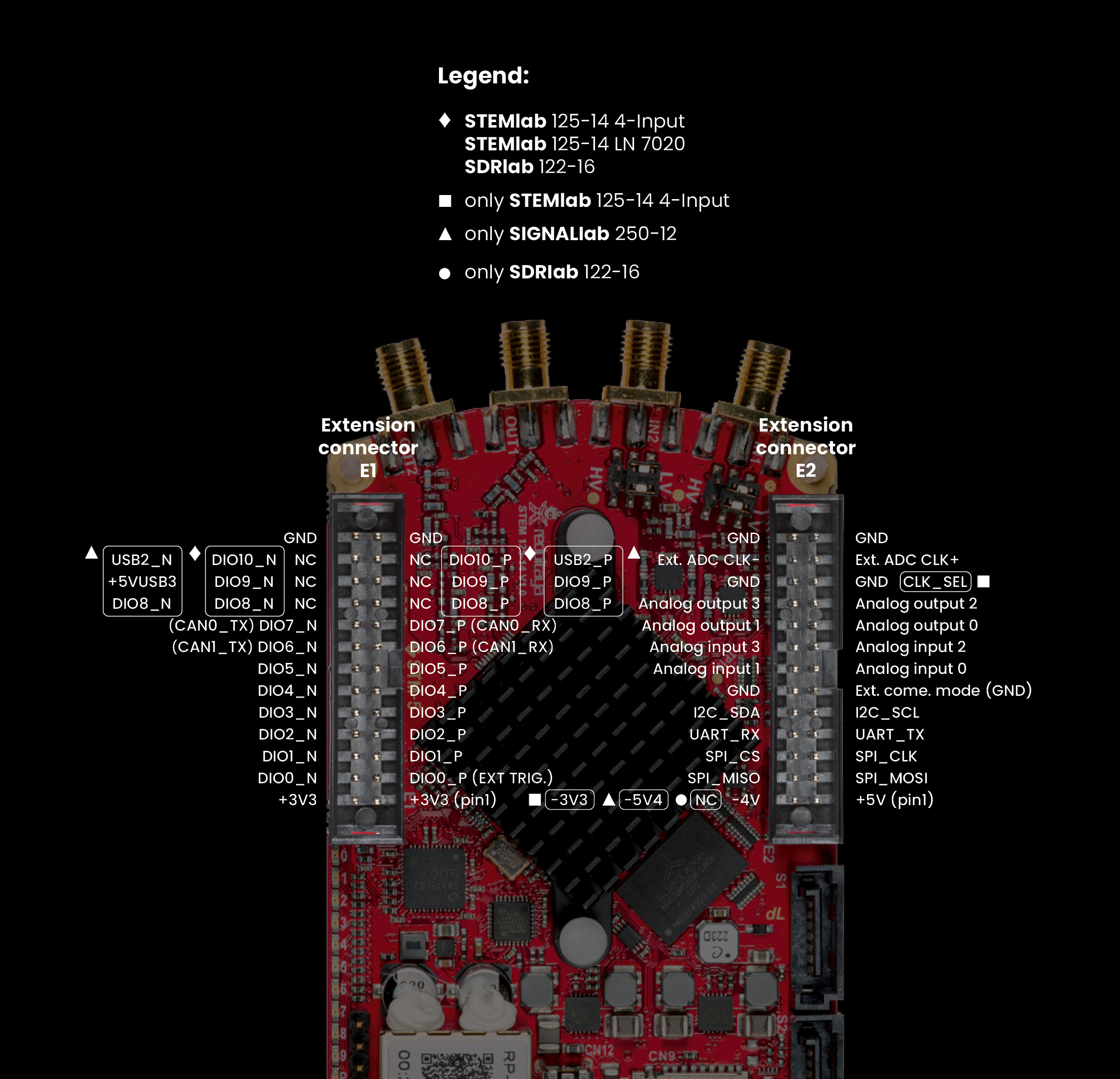
Extension Connectors & Interfaces
Overview
The SDRlab 122-16 board features the following connectors and interfaces:
E1 and E2 connectors: Primary expansion connectors with digital I/O, analog I/O, and communication interfaces. These connectors allow users to interface with additional hardware, sensors, or peripherals, enhancing the board’s capabilities.
S1 and S2 connectors: SATA connectors connected directly to the FPGA. Unlike the STEMlab 125-14, this board does not support multi-board clock synchronisation through these connectors — the shared clock signal does not propagate to the ADC and DAC. They can still be used to exchange clock, trigger, or data signals between boards or external devices. Note that the voltage levels are 1V8, which is non-standard for SATA connections.
Connector Physical Specifications
E1 and E2 Extension Connectors:
Connector type: 2 x 13 pins IDC 2.54 mm pitch
Pin count: 26 pins each (2x13 configuration)
Pitch: 2.54 mm (0.1”)
Mating Connectors:
Note
When looking for mating connectors for custom Red Pitaya shields, double height elevated sockets are needed to clear the heatsink and ethernet connector on the board. Any connectors with insulation height of 0.635” (16.13 mm) or greater will work. This clearance requirement is based on the tallest components on the Red Pitaya board (heatsink and ethernet connector).
Note
To prevent damage to the board or the shield, when connecting shields to the E1 and E2 connectors, please ensure:
Proper alignment of connectors - ensure the connectors are correctly aligned. The connectors on the Red Pitaya board have additional space in the socket housing, making it possible to misalign the shields by ±1 pin while still appearing physically connected. This can cause damage to the board and/or the shield, so please double-check the alignment before powering on the board.
Tight-fitting counterparts - use connectors that fit securely to prevent accidental disconnections or damage.
E1 Connector - Digital I/O & CAN
The E1 extension connector provides digital I/O and CAN bus interfaces for control and communication applications.
Features:
Two +3V3 power sources (max 0.5 A of current)
22 single-ended or 8 differential digital I/Os with 3.3 V logic levels
Two CAN buses (configurable via software)
Electrical Specifications:
All DIOx_y pins are LVCMOS33, with the following absolute maximum ratings:
Min. voltage: -0.40 V
Max. voltage: 3.3 V + 0.55 V
Drive strength: < 8 mA
E1 Pinout:
Pin |
Description |
FPGA pin number |
FPGA pin description |
Voltage levels |
|---|---|---|---|---|
1 |
3V3 |
|||
2 |
3V3 |
|||
3 |
DIO0_P / EXT TRIG |
G17 |
IO_L16P_T2_35 |
3.3V |
4 |
DIO0_N / TRIG OUT |
G18 |
IO_L16N_T2_35 |
3.3V |
5 |
DIO1_P |
H16 |
IO_L13P_T2_MRCC_35 |
3.3V |
6 |
DIO1_N |
H17 |
IO_L13N_T2_MRCC_35 |
3.3V |
7 |
DIO2_P |
J18 |
IO_L14P_T2_AD4P_SRCC_35 |
3.3V |
8 |
DIO2_N |
H18 |
IO_L14N_T2_AD4N_SRCC_35 |
3.3V |
9 |
DIO3_P |
K17 |
IO_L12P_T1_MRCC_35 |
3.3V |
10 |
DIO3_N |
K18 |
IO_L12N_T1_MRCC_35 |
3.3V |
11 |
DIO4_P |
L14 |
IO_L22P_T3_AD7P_35 |
3.3V |
12 |
DIO4_N |
L15 |
IO_L22N_T3_AD7N_35 |
3.3V |
13 |
DIO5_P |
L16 |
IO_L11P_T1_SRCC_35 |
3.3V |
14 |
DIO5_N |
L17 |
IO_L11N_T1_SRCC_35 |
3.3V |
15 |
DIO6_P / CAN1_RX |
K16 |
IO_L24P_T3_AD15P_35 |
3.3V |
16 |
DIO6_N / CAN1_TX |
J16 |
IO_L24N_T3_AD15N_35 |
3.3V |
17 |
DIO7_P / CAN0_RX |
M14 |
IO_L23P_T3_35 |
3.3V |
18 |
DIO7_N / CAN0_TX |
M15 |
IO_L23N_T3_35 |
3.3V |
19 |
DIO8_P |
Y9 |
IO_L14P_T2_SRCC_13 |
3.3V |
20 |
DIO8_N |
Y8 |
IO_L14N_T2_SRCC_13 |
3.3V |
21 |
DIO9_P |
Y12 |
IO_L20P_T3_13 |
3.3V |
22 |
DIO9_N |
Y13 |
IO_L20N_T3_13 |
3.3V |
23 |
DIO10_P |
Y7 |
IO_L13P_T2_MRCC_13 |
3.3V |
24 |
DIO10_N |
Y6 |
IO_L13N_T2_MRCC_13 |
3.3V |
25 |
GND |
|||
26 |
GND |
Note
To change the functionality of DIO6_P, DIO6_N, DIO7_P and DIO7_N from GPIO to CAN, please modify the housekeeping register value at address 0x34. For further details, please refer to the FPGA register section.
The change can also be performed with the appropriate SCPI or API command. Please refer to the CAN commands section for further details.
E2 Connector - Analog & Communication
The E2 extension connector provides analog I/O and communication interfaces for sensor integration and data acquisition.
Features:
+5 V power source (max 0.5 A, shared with USB devices)
SPI, UART, I2C communication interfaces
4 slow ADCs (12-bit, 100 kS/s)
4 slow DACs (8-bit PWM, ≲ 3.2 MS/s)
E2 Pinout:
Pin |
Description |
FPGA pin number |
FPGA pin description |
Voltage levels |
|---|---|---|---|---|
1 |
+5V |
|||
2 |
NC |
|||
3 |
SPI (MOSI) |
E9 |
PS_MIO10_500 |
3V3 |
4 |
SPI (MISO) |
C6 |
PS_MIO11_500 |
3V3 |
5 |
SPI (SCK) |
D9 |
PS_MIO12_500 |
3V3 |
6 |
SPI (CS) |
E8 |
PS_MIO13_500 |
3V3 |
7 |
UART (TX) |
D5 |
PS_MIO8_500 |
3V3 |
8 |
UART (RX) |
B5 |
PS_MIO9_500 |
3V3 |
9 |
I2C (SCL) |
B13 |
PS_MIO50_501 |
3V3 |
10 |
I2C (SDA) |
B9 |
PS_MIO51_501 |
3V3 |
11 |
Ext com. mode (AIN) |
GND (default) |
||
12 |
GND |
|||
13 |
Analog Input 0 |
B19, A20 |
IO_L2P_T0_AD8P_35, IO_L2N_T0_AD8N_35 |
0-7.0 V |
14 |
Analog Input 1 |
C20, B20 |
IO_L1P_T0_AD0P_35, IO_L1N_T0_AD0N_35 |
0-7.0 V |
15 |
Analog Input 2 |
E17, D18 |
IO_L3P_T0_DQS_AD1P_35, IO_L3N_T0_DQS_AD1N_35 |
0-7.0 V |
16 |
Analog Input 3 |
E18, E19 |
IO_L5P_T0_AD9P_35, IO_L5N_T0_AD9N_35 |
0-7.0 V |
17 |
Analog Output 0 |
T10 |
IO_L1N_T0_34 |
0-1.8 V |
18 |
Analog Output 1 |
T11 |
IO_L1P_T0_34 |
0-1.8 V |
19 |
Analog Output 2 |
P15 |
IO_L24P_T3_34 |
0-1.8 V |
20 |
Analog Output 3 |
U13 |
IO_L3P_T0_DQS_PUDC_B_34 |
0-1.8 V |
21 |
GND |
|||
22 |
GND |
|||
23 |
NC |
|||
24 |
NC |
|||
25 |
GND |
|||
26 |
GND |
Note
UART TX (PS_MIO08) is an output only. It must be connected to GND or left floating at power-up (no external pull-ups)!
Auxiliary Analog Inputs & Outputs
Auxiliary Analog Input Channels
The E2 connector provides 4 auxiliary analog inputs for slow-speed measurements and sensor interfacing.
Parameter |
Value |
Units |
Notes |
|---|---|---|---|
Number of channels |
4 |
- |
|
ADC resolution |
12 |
bit |
|
Sampling rate |
100 |
kS/s |
|
Input voltage range |
0 - 7.0 |
V |
|
Input coupling |
DC |
- |
|
Connector |
Extension connector E2 connector |
- |
Pins 13, 14, 15, 16 |
Auxiliary Analog Output Channels
The E2 connector provides 4 auxiliary analog outputs using PWM with low-pass filtering.
Parameter |
Value |
Units |
Notes |
|---|---|---|---|
Number of channels |
4 |
- |
|
Output resolution |
8 |
bit |
|
Sampling rate |
≲ 3.2 |
MS/s |
|
Output bandwidth |
≈ 160 |
kHz |
|
Output voltage range |
0 - 1.8 |
V |
|
Output coupling |
DC |
- |
|
Output type |
Low pass filtered PWM |
- |
|
PWM time resolution |
8 |
ns |
(1/125 MHz) |
Connector |
Extension connector E2 connector |
- |
Pins 17, 18, 19, 20 |
General Purpose Digital I/O Channels
Parameter |
Value |
Units |
Notes |
|---|---|---|---|
Number of GPIOs |
22 |
- |
|
Digital voltage level |
3.3 |
V |
|
Abs. min. voltage |
-0.40 |
V |
|
Abs. max. voltage |
3.3 + 0.55 |
V |
|
Current limitation |
< 8 |
mA |
Drive strength |
Direction |
Configurable |
- |
|
Time resolution |
8.14 |
ns |
(1/122.88 MHz) |
Connector location |
Extension connector E1 connector |
- |
Synchronisation Connectors (S1 & S2)
The Original generation Red Pitaya boards feature SATA connectors that are connected directly to the FPGA. Unlike the STEMlab 125-14, this board does not support multi-board clock synchronisation through the SATA connectors — the shared clock signal does not propagate to the ADC and DAC, so true synchronisation is not achievable this way. The connectors can still be used to exchange clock, trigger, or data signals between boards or external devices.
Synchronisation Connectors:
Parameter |
Specification |
|---|---|
Connector type |
SATA |
Number of connectors |
2 (for daisy-chaining) |
Maximum data rate |
up to 500 Mb/s |
Purpose |
Clock and trigger sync |
Note
The SATA connectors use 1V8 logic levels, which is non-standard for SATA connections. They are not compatible with standard SATA storage devices. Exercise caution when connecting external devices to these connectors to avoid damaging the board.
Advanced Features
Power Supply
Red Pitaya boards can be powered through two methods:
Micro USB connector
+5V pin (pin 1) and GND pin (pin 25, 26) on the |E2| connector
Power Supply Specifications:
Parameter |
Specification |
|---|---|
Power supply voltage |
5 V |
Maximum current draw |
2.0 A |
Power supply type |
DC |
Note
The board’s maximum current draw is 2.0 A. The power supply may have a higher current rating — this will not cause any issues.
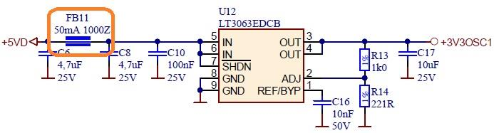
The micro-USB power input includes a simple integrated protection circuit that prevents damage to the board.
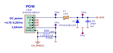
Figure 4.11 Protection circuit for powering through the micro-USB connector
Warning
When powering the Red Pitaya through the extension connector (+5V pin on E2 connector), external protection must be provided by the user to protect the board from overvoltage and overcurrent conditions.
Available Power Rails on Extension Connectors:
The E1 connector and E2 connector connectors expose several power rails that can be used to supply power to external devices or circuits connected to the board. The current limits below are the maximum currents that Red Pitaya can source from each rail to external loads — they are not related to the board’s own power consumption.
Voltage Rail |
Max. Sourceable Current |
|---|---|
+5 V |
0.5 A [6] |
+3V3 |
0.5 A [6] |
-3.3V / -3.4V / -4 V |
0.05 A |
Note
Exceeding these limits may cause voltage rail instability, which can result in a board reset or shutdown.
External ADC Clock
Note
The standard SDRlab 122-16 does not support external ADC clock without hardware modification. If you need external clock support without modification, use the pre-modified board:
SDRlab 122-16 External Clock — Board with external clock capability
Clock Sources
The ADC clock can be provided from two sources:
On-board 122.88 MHz oscillator (default): Internal clock source
External source through E2 connector: External clock via Ext. ADC Clk± pins (requires hardware modification described below)
External Clock Specifications
The external ADC clock should be a differential LVDS signal:
Parameter |
Description |
Min |
Typ |
Max |
Unit |
|
|---|---|---|---|---|---|---|
Clock input pins |
23 (Clk+) and 24 (Clk-) on E2 connector |
|||||
Input standards |
LVDS |
|||||
Input clock coupling |
AC (capacitors added during modification) |
|||||
\(f_{CLK}\) |
Input frequency range |
1 |
122.88 |
125 |
MHz |
|
\(V_{ID,DIFF,PP}\) |
Input voltage swing |
Differential peak-to-peak |
0.35 |
0.8 |
V |
|
IDC |
Input clock duty cycle |
45% |
55% |
|||
Required Materials
2x 100 nF 0402 capacitors
1x 100 Ω 0402 resistor
Hardware Modification Instructions
To enable external clock input, the following PCB modifications are required. Components crossed out with a red X in the images below are not placed on the standard SDRlab 122-16.
Move the 0R resistors R37 and R46 to positions R34 and R35.
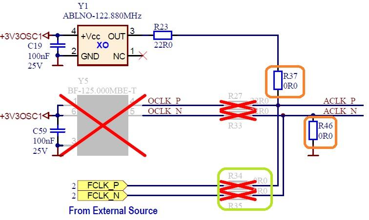
Remove the ferrite bead FB11.
Remove the 0R resistors on positions C64 and R24.
Add 100 nF 0402 capacitors to positions C64 and C63.
Add a 100 Ω resistor to position R36.
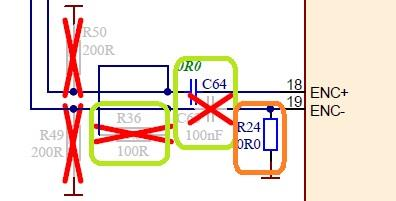
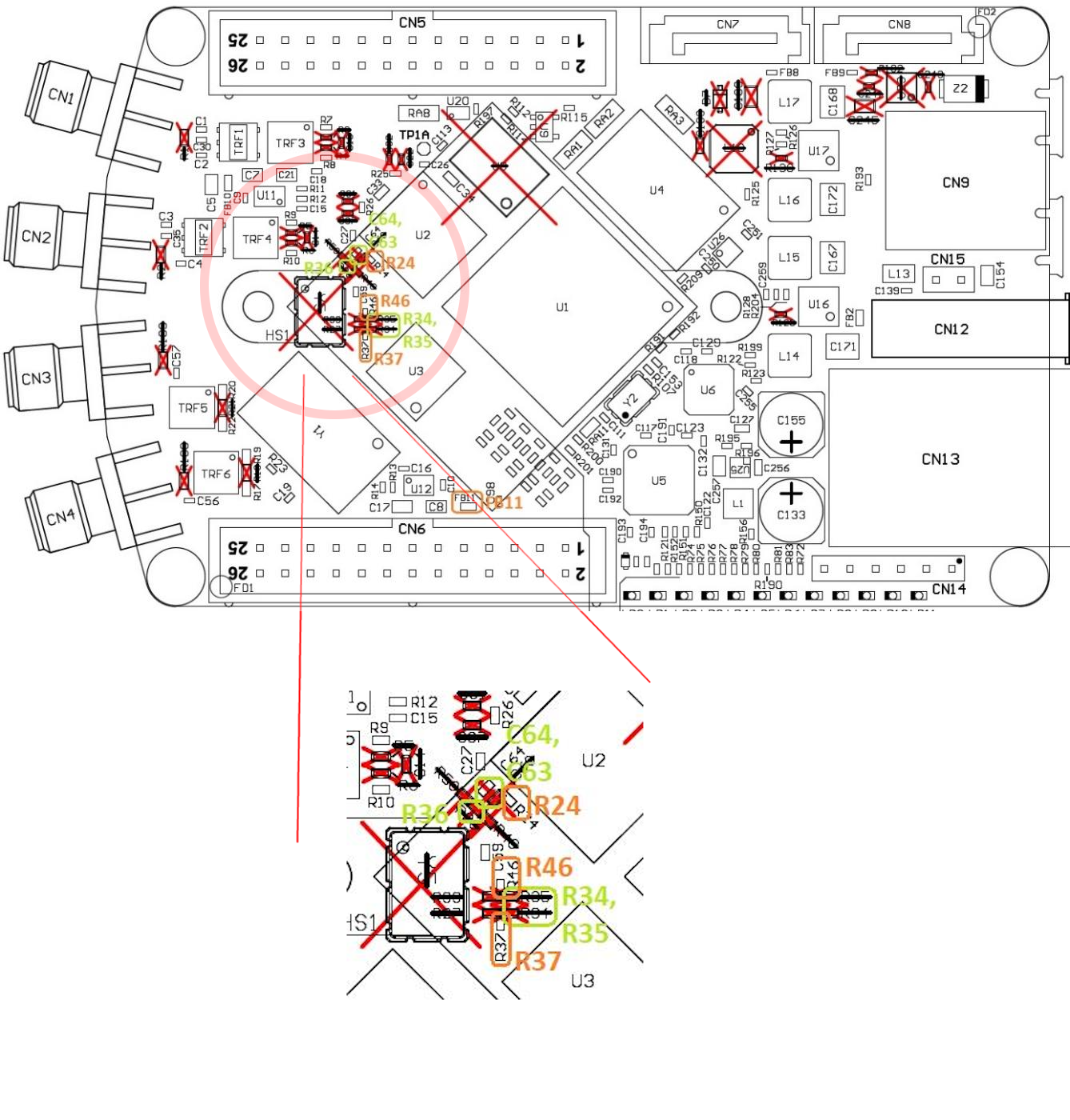
Figure 4.12 Full schematic showing modification positions
Warning
Changing the external clock frequency during operation is not supported
The Red Pitaya FPGA is designed, tested, and guaranteed to operate correctly at the board’s specified core clock frequency (122.88 MHz for SDRlab 122-16).
While it is possible to run the board at different clock frequencies, please be aware that:
The FPGA may not function as intended at non-standard frequencies and requires thorough testing
The ADC and DAC sampling rates will change proportionally with the clock frequency
Lower clock frequencies will reduce the analog bandwidth of the board
Red Pitaya does not guarantee proper operation at frequencies other than 122.88 MHz
The board will boot with any valid external clock signal. OS versions 2.07-48 and higher do not block boot-up if the external clock is absent.
Warning
Any non-Red Pitaya hardware modification will void the warranty, and we cannot guarantee support for modified boards.
QSPI Flash
The QSPI flash chip is by default not populated on Red Pitaya boards. For further information on board modifications, please contact support@redpitaya.com or info@redpitaya.com.
Warning
Any non-Red Pitaya hardware modification will void the warranty, and we cannot guarantee support for modified boards.
Calibration
Red Pitaya original generation boards are factory-calibrated. Recalibration may be required after extended use, environmental changes, or when measurement accuracy degrades.
There are three ways to calibrate the board:
Calibration application — graphical interface accessible from the System Tools menu. Recommended for most users.
Calibration command line utility (calib) — command line tool for scripted or advanced calibration workflows.
C++ or Python API commands — programmatic access to calibration parameters.
For a full description of the calibration procedure, required equipment, and technical reference, please refer to the Calibration documentation.
Note
Original generation boards require 50 Ω terminators during calibration due to a mismatch in the impedance of fast analog inputs and outputs.
Additional Resources
For additional specifications and measurements, please refer to:
Original Gen hardware specifications - Common Original Gen specifications
Original Gen board comparison table - Comparison across all Red Pitaya Original Gen models
SDRlab 122-16 External Clock - External clock variant
Legal & Disclaimers
Note
The information provided by Red Pitaya d.o.o. is believed to be accurate and reliable. However, no liability is accepted for its use. Please note that the contents may be subject to change without prior notice.
Footnotes