Base FPGA Project
The Base FPGA Project serves as the foundation for all tutorials in the FPGA series. This tutorial will guide you through setting up a custom FPGA component based on the Red Pitaya v0.94 project that simplifies the design by removing unnecessary complexity while maintaining essential functionality for learning FPGA development.
Overview
The tutorials in this series are built on a custom processing component (red_pitaya_proc) that replaces the PID controller in the standard v0.94 FPGA
project. The component is designed to be as versatile as possible by sitting in-line in both signal chains:
ADC signal chain — ADC data passes through
red_pitaya_procbefore reaching the Oscilloscope module. By default this is a passthrough, but you can insert your own processing logic.DAC signal chain — The ASG (Arbitrary Signal Generator) output passes through
red_pitaya_procbefore reaching the physical DAC. By default this is also a passthrough.System bus interface — Register-based control from Linux
GPIO control — Full access to expansion connector digital I/O
LED control — Status indication and debugging
This design allows you to intercept and modify both the ADC and DAC signal paths without changing the top-level wiring, making it straightforward to add processing logic in later tutorials. When no logic is added, all signals pass through unmodified and the board behaves identically to the standard v0.94 project.
Prerequisites
Before starting this tutorial, you should:
Complete the Creating an FPGA project in Vivado tutorial
Have a working Vivado installation with the v0.94 project
Understand basic Verilog or VHDL syntax
Be familiar with the v0.94 FPGA project structure
Board compatibility:
All Red Pitaya board models
What This Base Project Includes
The base project for these tutorials uses a simplified signal path compared to the production v0.94 FPGA:
Included:
Direct ADC data from IN1/IN2 (14-bit signed samples)
Direct DAC control to OUT1/OUT2 (14-bit signed output)
System bus interface for register access
GPIO and LED control
Clock and reset signals
NOT Included (Intentionally Simplified):
Board calibration circuits - The production Oscilloscope and ASG modules contain frequency equalisation filters and gain/offset calibration. These are bypassed in tutorials for simplicity.
Decimation and averaging filters - The Oscilloscope module’s built-in filtering
Trigger logic - Oscilloscope triggering mechanisms
DMA and deep memory - Advanced data capture features
Of course, we will cover how to implement a simplified version of these features in later tutorials, but the base project focuses on the core FPGA concepts without the additional complexity of the full production design.
Warning
Important: Calibration Implications
The tutorials bypass the v0.94 project’s calibration system, which consists of:
Oscilloscope module (i_scope): Digital equalisation filter + gain/offset correction
Signal Generator module (i_asg): Gain/offset calibration on outputs
This means tutorial projects will not have the same measurement accuracy as production applications. The raw ADC/DAC signals are used directly. This is intentional to keep tutorials focused on fundamental FPGA concepts.
For production applications, you should either:
Implement your own calibration based on EEPROM values (can be a copy of the existing v0.94 approach) - Recommended
Use the existing Scope/ASG modules with calibration
Accept the reduced accuracy for non-critical applications
Creating the Custom Component
The custom red_pitaya_proc component is fully documented in the Adding a custom component section of the Getting Started
guide.
To create the base project:
Follow the complete tutorial at Adding a custom component
This will guide you through:
Removing the PID controller from v0.94
Creating the custom component with VHDL or Verilog
Connecting ADC/DAC signals directly
Wiring up GPIO and LED control
Implementing the system bus interface
The resulting project will have the custom component connected to:
System bus section 3 (address
0x40300000to0x403FFFFF)ADC data buses — component sits between the ADC and the Oscilloscope module
DAC data buses — component sits between the ASG and the physical DAC output
GPIO expansion connector pins
LED outputs
Note
In-line signal path
red_pitaya_proc sits in-line in both chains. The default implementation is a pure passthrough:
// ADC passthrough (Verilog)
assign adc_a_out = adc_a_in;
assign adc_b_out = adc_b_in;

// DAC passthrough — ASG signal passes through unchanged
assign dac_a_out = dac_a_in;
assign dac_b_out = dac_b_in;
In tutorials you will replace these assignments with your own logic to process or generate signals. Because the component is already wired into both chains, no top-level changes are needed to start processing — just replace the passthrough assignments.
Custom Component Register Map
The red_pitaya_proc component implements the following register interface at base address 0x40300000:
Address |
Register |
Access |
Description |
|---|---|---|---|
0x00000 |
ID |
R |
Component ID (0xFEEDBACC) |
0x00010 |
GPIO_P_DIR |
R/W |
GPIO P row direction (0=input, 1=output) |
0x00014 |
GPIO_N_DIR |
R/W |
GPIO N row direction (0=input, 1=output) |
0x00018 |
GPIO_P_OUT |
R/W |
GPIO P row output data |
0x0001C |
GPIO_N_OUT |
R/W |
GPIO N row output data |
0x00020 |
GPIO_P_IN |
R |
GPIO P row input data |
0x00024 |
GPIO_N_IN |
R |
GPIO N row input data |
0x00030 |
LED |
R/W |
LED control (8 bits) |
Access these registers from Linux using the monitor utility:
# Read component ID
monitor 0x40300000

# Set LED pattern
monitor 0x40300030 0xFF
Signal Flow Diagram
Understanding the signal path in the base project:
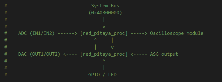
red_pitaya_proc sits in-line in both chains. By default signals pass straight through.
You add processing logic inside the component, with no top-level wiring changes required.
The key difference from production v0.94:
Production path: ADC → Gain/Offset Calibration → Equalisation Filter → Averaging & Decimation → Scope Buffer
Tutorial path: ADC → Direct to custom component
Next Steps
Once you have created the base project with the custom component:
Verify the build - Ensure synthesis, implementation, and bitstream generation complete successfully
Test the component - Load the bitstream and verify register access
Explore tutorials - Move on to the specific FPGA lessons
Each tutorial builds upon this base project, adding functionality to the custom component or creating new modules that interact with it.
Troubleshooting
Synthesis errors after adding custom component:
Verify all port widths match between
red_pitaya_topandred_pitaya_procCheck that
DWEparameter is correctly passed (GPIO width varies by board model)Ensure the custom component file is not disabled in Design Sources
No output on DAC:
By default the DAC output is the ASG signal passed through unchanged. If the ASG is disabled and the passthrough assignments are not replaced with your own logic, the DAC output will be zero.
Verify the output value is within the 14-bit signed range
Check that the register writes are reaching the component
GPIO not responding:
GPIO direction must be set to output (1) for pins to drive
LED and GPIO control through SCPI/API will not work (disconnected from housekeeping)
Additional Resources
Full custom component implementation: Adding a custom component
v0.94 project details: FPGA project v0.94
System bus architecture: System bus
Board-specific variations: Check your board model documentation