FAQ Gen 2
Here are some frequently asked questions about the Red Pitaya Gen 2 boards.
Fast analog inputs and outputs
Where can I find the measurements for the fast analog frontend?
Measurements for the fast analog frontend on Gen 2 boards can be found in the Performance & Measurements chapter under each board specifications.
How to bypass input FPGA filter on Gen 2 boards?
The easiest way to bypass the input FPGA filter on Gen 2 boards is to disable it in the Oscilloscope application input settings.
Alternatively, the reconstruction filter can be disabled by modifying the register value of the Reconstruction filter bypass register (address 0x4010_0098) in the FPGA image. You can find the register description in the FPGA registers section.
How can I make sure Red Pitaya outputs are at 0 V when Red Pitaya is booting?
The output signal on Gen 2 boards is disabled by hardware until the FPGA image has finished loading. Afterwards, how the DAC is configured (initialised) in the FPGA image determines the output signal. To prevent output voltage spikes, the DAC should be initialised to 0 V.
As the official Red Pitaya OS image needs to identify the type of Red Pitaya board first, the DAC is not initialised immediately. Consequently, there will be a spike at the outputs after the FPGA image has loaded, until the DAC is initialised.
External clock and synchronisation
Where can I find the external clock specifications?
The external ADC clock should comply with NB6L72 input specifications. The chip is powered by 3V3.
How to switch from internal to external clock?
The main FPGA CLK signal on STEMlab 125-14 PRO Gen 2 and STEMlab 125-14 PRO Z7020 Gen 2 boards can be supplied from an external source through the Ext. ADC Clk± ports.
Both the internal oscillator clock and the external clock signal are connected to the NB6L72 Differential Crosspoint Switch. The CLK_SEL pin is used to select the clock source:
3V3 (logic high) or unconnected - Internal clock.
GND (logic low) - External clock.
The clock signal then travelles from the output of the NB6L72 through the ADC to the FPGA.
External clock specifications The external ADC clock should comply with NB6L72 input specifications. The chip is powered by 3V3.
Note
When synchronising multiple Red Pitaya PRO Gen 2 boards, please keep in mind that:
X-channel 2.0 (Click Shield) synchronisation works out-of-the-box.
X-channel synchronisation requires a hardware modification as secondary boards differ from the primary board.
Note
Switching between internal and external clock is only available on the Gen 2 PRO board models (STEMlab 125-14 PRO Gen 2, STEMlab 125-14 PRO Z7020 Gen 2).
How to synchronise Gen 2 boards (multichanneling)?
The Gen 2 boards can be syncrhonised in the same way as original boards:
X-channel 2.0 (Click Shield) synchronisation works out-of-the-box.
X-channel synchronisation requires a hardware modification as secondary boards differ from the primary board. Also USB-C cables are used for synchronisation instead of SATA cables.
How to synchronise Gen 2 boards over USB-C daisy chain connection?
Connect the two boards together with a USB-C data cable. Make sure that the Orientation and Link LEDs are lit.
Please check the X-channel synchronisation section for more information.
Can I connect other devices to the USB-C daisy chain connectors?
No, the USB-C daisy chain connectors do not meet the USB-C standard and are only meant for synchronisation between multiple Red Pitaya boards. Connecting other devices may damage the board. For connecting peripherals, use the dedicated USB-C connector (labelled HOST) on the bottom side of the board.
E3 connector and QSPI eMMC module
Where can I find the E3 connector pinout?
Check the E3 connector pinout section for more information.
Are the fast differential pair votage levels configurable? What should I watch out for?
The fast differential pair voltage levels are determined by the power supply voltage on Bank 13 of Zynq 7020 FPGA. By default, the votlage is set to 2.5 V, but can be configured between 2.5 V and 3.3 V by changing the position of the ferrite bead from position FB26 to position FB25 on the PCB.
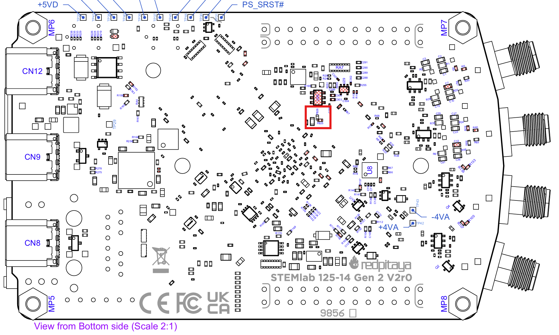
Figure 4.1 Fast differential pairs power supply configuration
To utilise the full speed of the fast differential pairs, Bank 13 voltage should be set to 2.5 V.
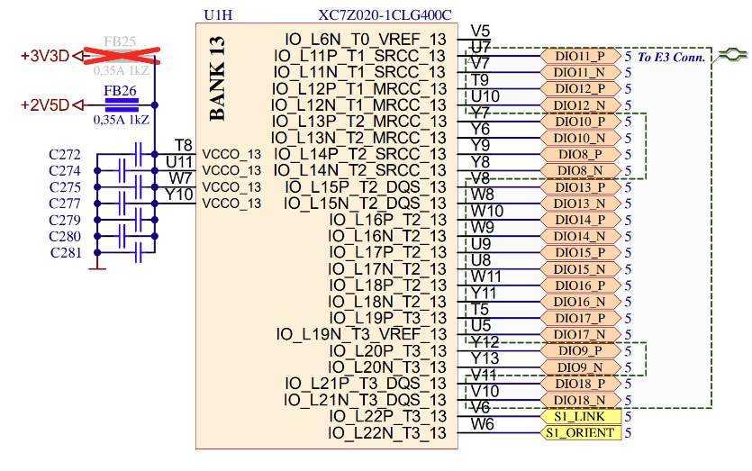
Figure 4.2 Bank 13 of Zynq 7020 FPGA
List of Bank 13 pins |
Connector |
Type |
|---|---|---|
DIO8_P, DIO8_N |
E1 |
Input/Output |
DIO9_P, DIO9_N |
E1 |
Input/Output |
DIO10_P, DIO10_N |
E1 |
Input/Output |
DIO11_P, DIO11_N |
E3 |
Input/Output |
DIO12_P, DIO12_N |
E3 |
Input/Output |
DIO13_P, DIO13_N |
E3 |
Input/Output |
DIO14_P, DIO14_N |
E3 |
Input/Output |
DIO15_P, DIO15_N |
E3 |
Input/Output |
DIO16_P, DIO16_N |
E3 |
Input/Output |
DIO17_P, DIO17_N |
E3 |
Input/Output |
DIO18_P, DIO18_N |
E3 |
Input/Output |
S1_LINK |
S1 Link LED |
Input |
S1_ORIENT |
S1 Orientation LED |
Input |
Note
Changing the power supply of Bank 13 affects the digital voltage levels of all the pins connected to it. This includes not only the fast differential pairs, but also the DIO10-DIO8 GPIO pins on the E1 extension connector.
Where can I find the documentation for the QSPI eMMC (E3) module?
Check the QSPI eMMC module section for more information.
My Gen 2 board does not boot with the QSPI eMMC module connected. What should I do?
When the QSPI eMMC module is connected to the Red Pitaya board, Red Pitaya will not boot automatically. The P-ON button on the QSPI eMMC module should be pressed to power up the Red Pitaya board.
Check the QSPI eMMC module section for more information.
Power supply
How can I disable Power Delivery negotiation when using a USB-C power supply?
Jumper JP5 located near S1 and S2 synchronisation connectors disables the Power Delivery negotiation. Connecting the two pads with a solder bridge will disable the Power Delivery negotiation.
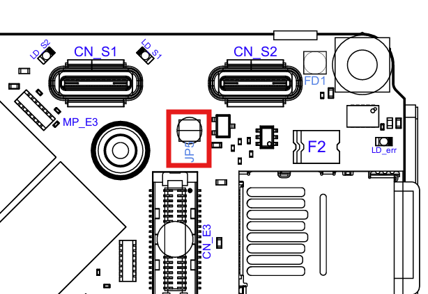
Figure 4.3 JP5 position to disable Power Delivery negotiation
Other
Where can I find Gen 2 board schematics?
Board development schematics are available in the Schematics & 3D Models chapter under each board model hardware specification section.
Where can I find Gen 2 board 3D models?
3D models of Red Pitaya boards are available in the Schematics & 3D Models chapter under each board model hardware specification section.