Modifying the FPGA project
Project modification can include changing the functionality of the design, adding new features, or fixing bugs. In this guide, we will focus on modifying the existing v0.94 FPGA project to change the behavior of the LED output and adding our own component. These two modifications will help you understand the process of working with FPGA projects and how to adapt them to your needs.
Prerequisites
This example project doesn’t have any specific prerequisites, but familiarity with Verilog and FPGA design concepts will be helpful.
Board model compatibility:
All Red Pitaya boards
Based on:
If you are looking for detailed description of the v0.94 FPGA project, click on the link above.
Note
Since Red Pitaya board models have slightly different variations of the v0.94 FPGA project due to the nature of the hardware, the exact code lines mentioned in the tutorial may differ slightly.
Removing extra design source files
In this step, we will remove any unnecessary design source files from the project to keep it clean and organized.
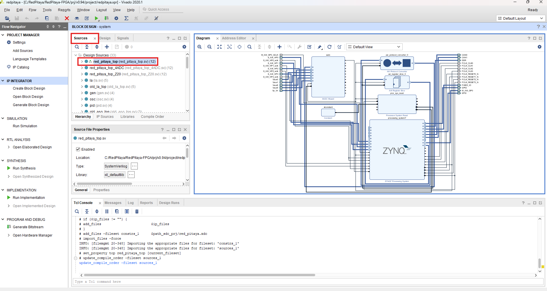
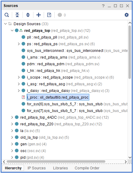
Locate Design Sources: Inside the Sources panel in Vivado, locate the Design Sources directory.
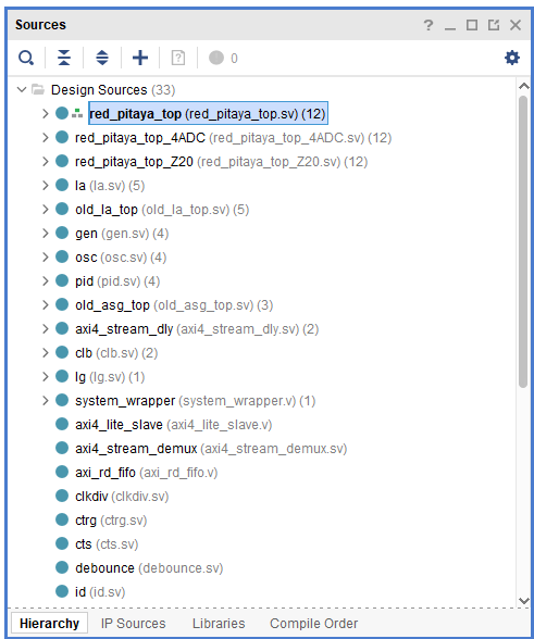
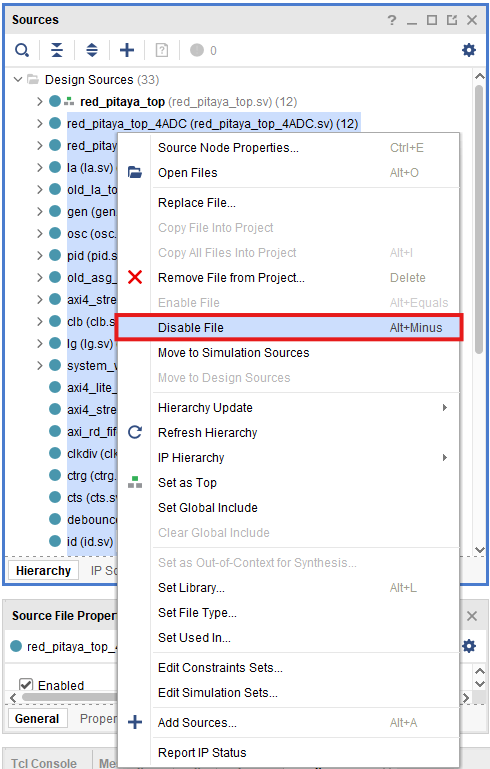
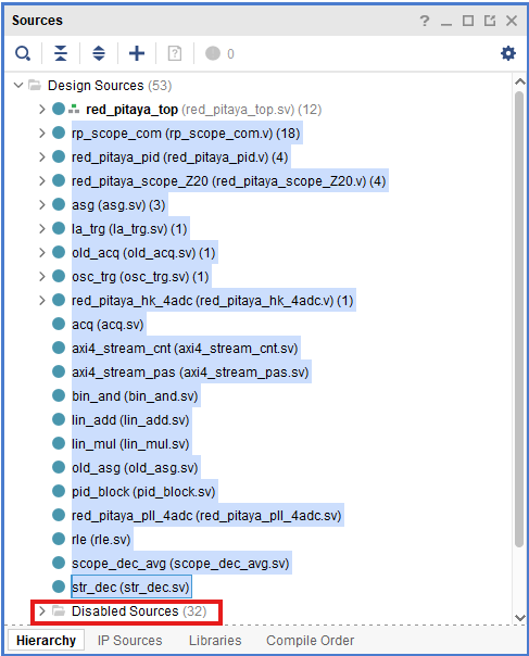
Disable Unnecessary Files: As we can see, the Design Sources contains a lot of different Verilog files, of which most are not needed in the v0.94 project (most of the files contain old functionality or alternative functionality of v0.94 project for different board models). The only file tree related to our project is at the top of the list, written in bold, with a small pyramid next to it. Shift Select all the other files. Right-click and select Disable file to “exclude” them from the project.
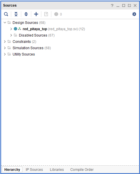
Repeat for Tree-Like Structures: As most of the disabled files have a tree-like file structure, repeat step number 2 until only the red_pitaya_top file tree remains.
Simple LED blink
In this project modification, we will focus on taking one of the existing signals, specifically the LEDs, and modifying its behavior.
To start, open the Vivado project you created in the previous section. If you haven’t created a project yet, please refer to the Creating an FPGA project in Vivado section.
To make things simple, we will only edit the top-level module red_pitaya_top.sv and work with existing signals.
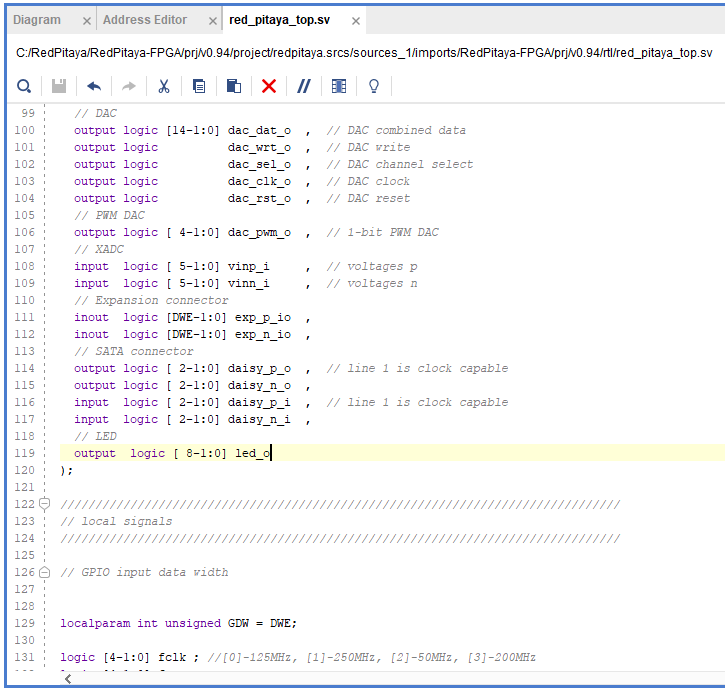
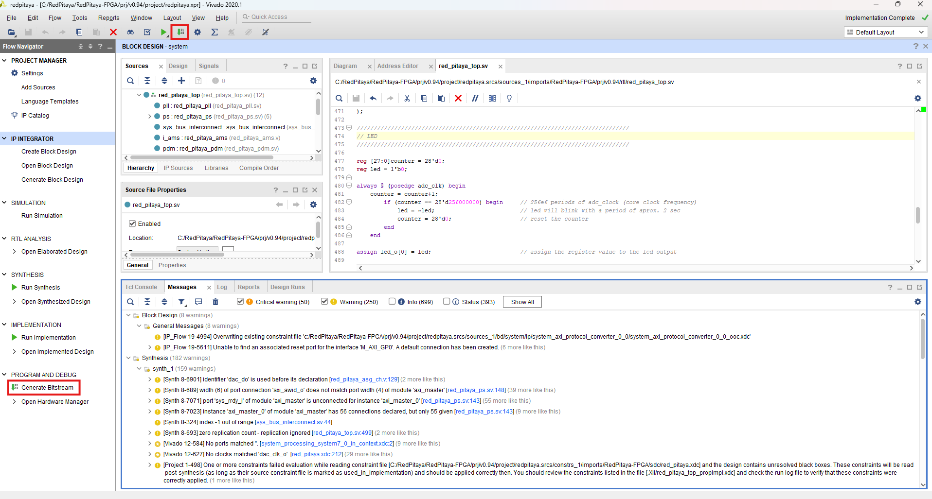
Open the Top-Level Module: Open the red_pitaya_top.sv file. Go to the Sources panel in Vivado, and locate the red_pitaya_top.sv file under the Design Sources directory. Double-click the name to open it in the editor.
Modify the LED Port: Change the led_o port in top level module/entity in line 119 from inout logic to output logic. This change will allow us to control the LED output directly from the FPGA design and skip the complicated three-state logic.
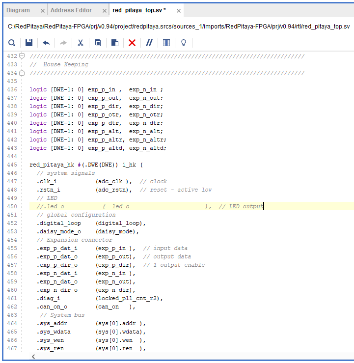
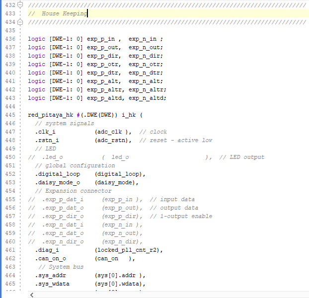
Comment the LED Port in House Keeping Section: Scroll down to the House Keeping section. We can also use Ctrl+F to search for the keyword House Keeping. This section contains the code that manages the LEDs and GPIOs. Comment the led_o port.
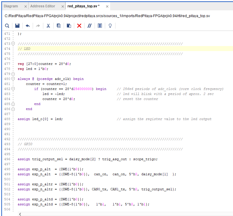
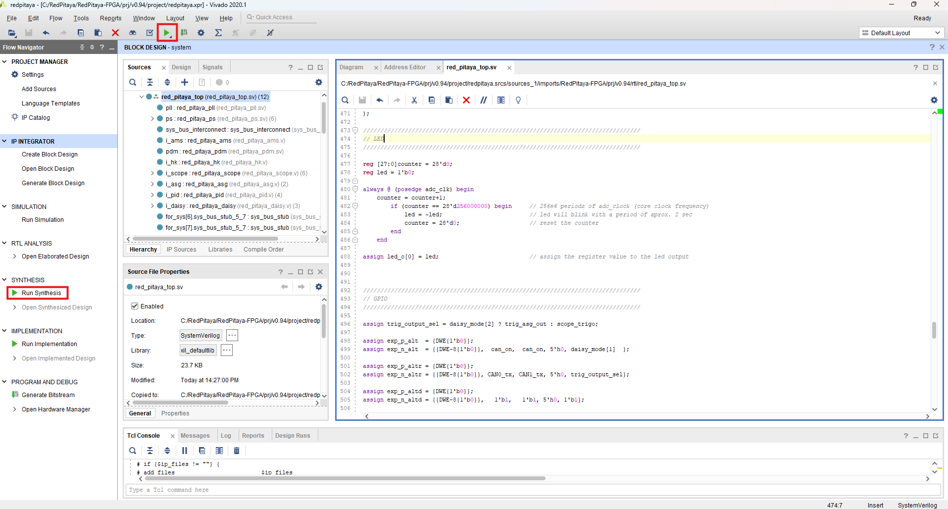
Insert LED Blink Code: Scroll down a bit further to get to the empty LED section. Insert the following code to make the LED 0 blink
reg [27:0]counter = 28'd0;
reg led = 1'b0;

always @ (posedge adc_clk) begin
    counter = counter+1;
    if (counter == 28'd256000000) begin      // 256e6 periods of adc_clock (core clock frequency)
        led = ~led;                          // led will blink with a period of aprox. 2 sec
        counter = 28'd0;                     // reset the counter
    end
end

assign led_o[0] = led;                       // assign the register value to the led output
As the counter increases with the core clock frequency of the Red Pitaya unit, the blink period will vary depending on the board model:
2.083 seconds (for 122.88 MHz)
2.048 seconds (for 125 MHz)
1.024 seconds (for 250 MHz)
To adjust the blink period, change the value in the if (counter == 28’d256000000) line.
Save the Changes: Save the changes by clicking on the Save icon in the toolbar or using the shortcut Ctrl+S.
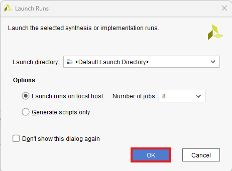
Synthesize the Design: Now that we have modified the code, we need to synthesize the design to check for any errors. Click on the Run ==> Synthesis button (green play button) in the toolbar or click on the Run Synthesis option in the Flow Navigator panel on the far left.
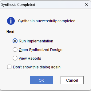
Review Synthesis Results (optional): After the synthesis is complete, Vivado will display a summary of the synthesis results. If there are no errors, we can proceed to the next step. If there are errors, review the messages in the Synthesis panel and fix them accordingly. During the build process, Vivado will also check for any warnings or errors in the code. If there are any issues, they will be displayed in the Messages panel at the bottom of the Vivado window. During the build of the v0.94 project, Vivado will report a few warnings, which can be safely ignored.
Open Synthesized Design: When the synthesis is finished, a window will pop up with the synthesis results and an option to proceed with implementation. If you are curious, click on the Open Synthesized Design button to open the synthesized design in the Vivado editor.
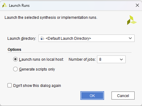
Run Implementation: We will proceed with the implementation step. Similarly to launching the synthesis, click on the Run ==> Implementation button (green play button) in the toolbar, click on the Run Implementation option in the Flow Navigator panel on the far left or select Run implementation option from the synthesis result pop-up.
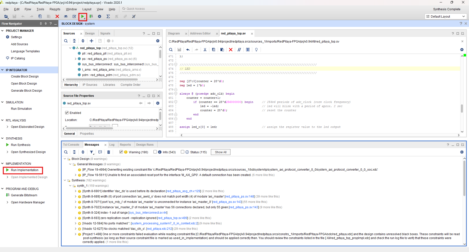
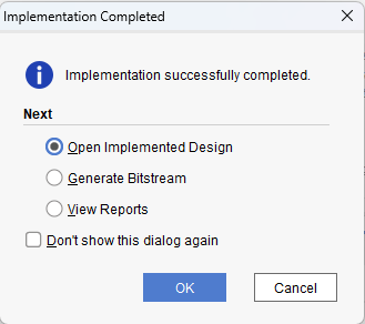
Review Implementation Results (optional): After the implementation is complete, Vivado will display a summary of the implementation results. If there are no errors, we can proceed to the next step. If there are errors, review the messages in the Implementation panel and fix them accordingly. During the build process, Vivado will also check for any warnings or errors in the code. If there are any issues, they will be displayed in the Messages panel at the bottom of the Vivado window. During the build of the v0.94 project, Vivado will report a few warnings, which can be safely ignored.
Generate Bitstream: The final step is bitstream generation, which can be launched from the Program and Debug section in the Flow Navigator or the Generate Bitstream button in the toolbar.
Note
Generate Bitstream Directly: What we haven’t mentioned is that you can also generate the bitstream file directly from the start. In this case Vivado will automatically run synthesis, implementation, and bitstream generation in one go, informing us of any additional steps that need to be taken.
Review Bitstream Generation Results: Once bitstream generation is complete, the following pop-up window will appear. If you are curious you can explore the different options, but for now, close the pop-up.
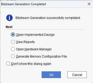
Locate the Bitstream File: The bitstream file is named after the top module red_pitaya_top.bit and located in the /prj/v0.94/project/repitaya.runs/impl_1 directory of the downloaded Red Pitaya FPGA Repository.
The next step is transfering the bitstream to the Red Pitaya board and loading it into the FPGA. For this, please refer to the Reprogramming the FPGA section.
Adding a custom component
To start, open the Vivado project you created in the previous section. If you haven’t created a project yet, please refer to the Creating an FPGA project in Vivado section.
Here, we will focus on adding a custom component/module named red_pitaya_proc to the existing v0.94 FPGA project and reroute the existing signals to it. This will help you understand how to integrate your own designs into the Red Pitaya FPGA project structure. The source and HDL language used to describe the custom component itself is not important as the nature of HDL languages enables us to view each module as a black box with defined input and output ports. As long as the “black box” has the expected ports (matching name, width and direction), it can be integrated into the existing design.
Our custom component will have the following functionality:
System bus connection. This will allow the component to communicate with the Red Pitaya system bus and receive commands from the host.
ADC. Interface with the ADC to receive input signals from IN1 and IN2 for processing.
DAC. Interface with the DAC to send processed output signals to OUT1 and OUT2.
GPIOs. Use GPIOs for general-purpose input/output operations.
LEDs. Control LEDs for status indication and debugging purposes.
As discussed in v0.94 FPGA project description, the system bus on Red Pitaya is split into eight sections. Generally, we could have connected the custom component to one of the free sections, but for this example, we will be replacing the existing PID component.
Changes to red_pitaya_top
Removing an existing component: Removing an existing component is straightforward - we only have to remove the code that connects the unwanted component to the top module. In the red_pitaya_top.sv file, locate the MIMO PID controller section and comment out the entire section.
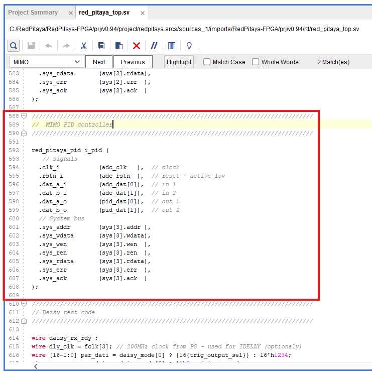
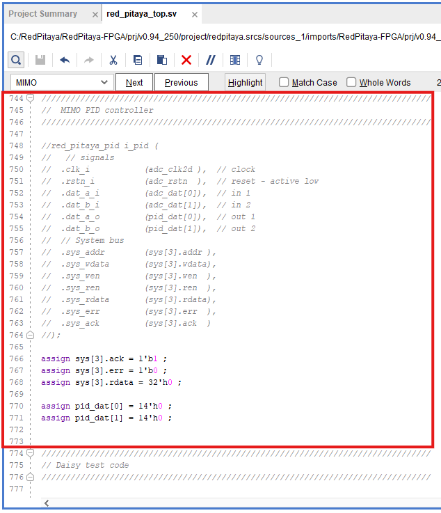
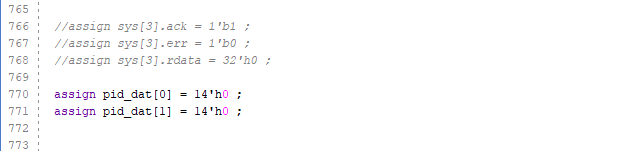
In some projects (for example, v0.94_250 meant for SIGNALlab 250-12), the PID component is already commented out, but there are a few lines of code that ensure the correct functionality of the system bus. Comment out the lines related to system bus, but leave the pid_dat signals intact. If we take a closer look at the signals connected to the PID component, we can already guess which signals will need to be connected to our custom component.
Add a custom component connection: We will add the custom component connection to the very end on the red_pitaya_top.sv file, just before the final endmodule statement. To start, we can copy over the existing PID component instantiation, which we will slowly modify to match our custom component’s interface.
red_pitaya_proc #(
    // Generic parameters

)
i_proc(
    // Signals
    .clk_i          (adc_clk         ), // clock
    .rstn_i         (adc_rstn        ), // reset - active low

    // ADC
    .dat_a_in       (                ), // IN 1
    .dat_b_in       (                ), // IN 2

    // DAC
    .dat_a_out      (                ), // OUT 1
    .dat_b_out      (                ), // OUT 2

    // System bus
    .sys_addr       (sys[3].addr     ), // System address
    .sys_wdata      (sys[3].wdata    ), // Write data
    .sys_wen        (sys[3].wen      ), // Write enable
    .sys_ren        (sys[3].ren      ), // Read enable
    .sys_rdata      (sys[3].rdata    ), // Read data
    .sys_err        (sys[3].err      ), // Error
    .sys_ack        (sys[3].ack      ), // Acknowledge
);
As there are quite a few changes we need to make, we will go through them step by step.
GPIO and LEDs
By default, the GPIOs and LEDs are connected to the House Keeping module (red_pitaya_hk). We will have to disconnect them from there and connect them to our custom component instead.
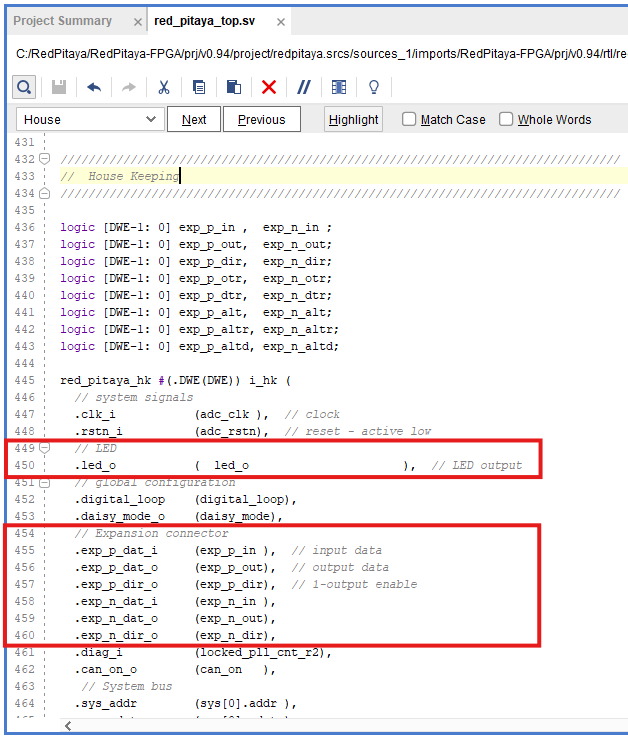
The digital pins on the E1 connector are connected directly to the FPGA. Inside the FPGA, they first connect to an input-output buffer, which splits each pin’s signal into three digital signals:
Input data
Output data
Direction control (0 = input, 1 = output)
Furthermore, since there are two rows of GPIO pins, which can be treated as differential pairs (labelled P and N), this results in a grand total of 6 GPIO signals:
exp_p_in- input data for the P rowexp_p_out- output data for the P rowexp_p_dir- direction control for the P rowexp_n_in- input data for the N rowexp_n_out- output data for the N rowexp_n_dir- direction control for the N row
Each of these signals’ widths corresponds to the number of GPIO pins on the E1 connector (usually either 8 or 11). Each bit represents a single GPIO pin in the corresponding row (the LSB is pin 0).
Copy the GPIO and LED signals to custom component: Copy the GPIO and LED signal connections from the House Keeping section and paste them into the custom component instantiation. The GPIOs will be connected to the exp_p_in, exp_p_out, exp_p_dir, exp_n_in, exp_n_out, and exp_n_dir signals, while the LEDs will be connected to the led_o signal. Then comment out the original connections in the House Keeping section.
Add generic parameter for GPIO width: We will also add a generic parameter DW (digital width) to determine the width of the GPIO signals. This will allow us to easily adapt the component to different board models with varying numbers of GPIO pins.
Here is how our custom component instantiation should look like so far:
red_pitaya_proc #(
    // Generic parameters
    .DW             (DWE             )  // GPIO bus width
)
i_proc(
    // Signals
    .clk_i          (adc_clk         ), // clock
    .rstn_i         (adc_rstn        ), // reset - active low

    // ADC
    .dat_a_in       (                ), // IN 1
    .dat_b_in       (                ), // IN 2

    // DAC
    .dat_a_out      (                ), // OUT 1
    .dat_b_out      (                ), // OUT 2

    // GPIO + LED
    .led_o          (led_o           ), // LED output
    .gpio_p_i       (exp_p_in        ), // GPIO P row input
    .gpio_p_o       (exp_p_out       ), // GPIO P row output
    .gpio_p_dir     (exp_p_dir       ), // GPIO P row direction
    .gpio_n_i       (exp_n_in        ), // GPIO N row input
    .gpio_n_o       (exp_n_out       ), // GPIO N row output
    .gpio_n_dir     (exp_n_dir       ), // GPIO N row direction

    // System bus
    .sys_addr       (sys[3].addr     ), // System address
    .sys_wdata      (sys[3].wdata    ), // Write data
    .sys_wen        (sys[3].wen      ), // Write enable
    .sys_ren        (sys[3].ren      ), // Read enable
    .sys_rdata      (sys[3].rdata    ), // Read data
    .sys_err        (sys[3].err      ), // Error
    .sys_ack        (sys[3].ack      ), // Acknowledge
);
ADC and DAC
Now we will configure the ADC and DAC connections. The ADC and DAC signals are already defined in the top module, so we just need to connect them to our custom component.
Note
Some Red Pitaya board models (for example STEMlab 125-14 4-Input) have a different number of ADC and DAC channels. The code snippets in this tutorial are based on the 2-channel configuration, but they can be easily adapted to different board models by changing the signal names and widths accordingly. For example, for 4-channel ADC configuration, create 4 input ports in the custom component and connect them to the corresponding ADC signals in the top module.
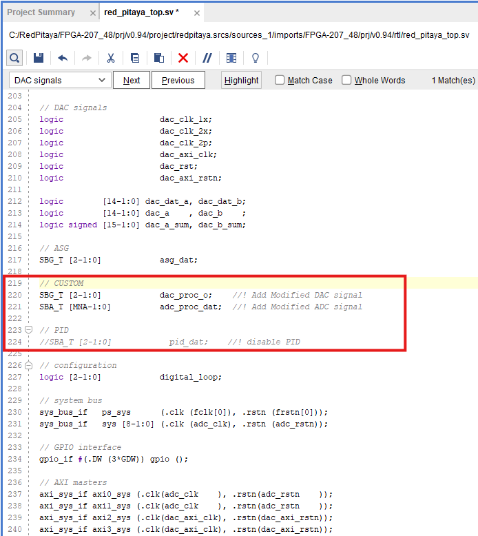
Add new ADC and DAC busses: First, we will add a new bus for the ADC and DAC signals, which will replace the
pid_datas the output of our component. Add the following lint near the ASG and PID bus declarations (around line 200). At the same time comment out the original PID bus declaration.// CUSTOM SBG_T [2-1:0] dac_proc_o; //! Add Modified DAC signal SBA_T [MNA-1:0] adc_proc_dat; //! Add Modified ADC signal // PID //SBA_T [2-1:0] pid_dat; //! disable PID
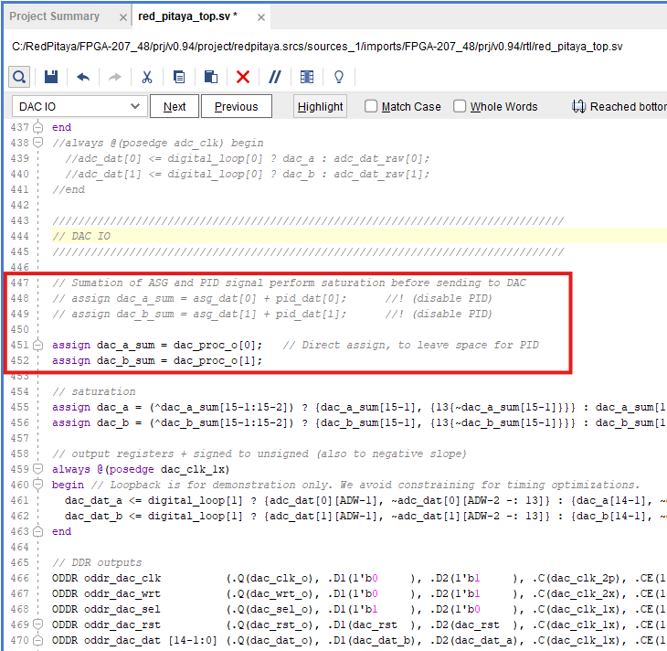
Remove the PID signals: Next, we will remove the existing PID signals and connect the custom DAC bus in their place. This will allow us to send the processed output signals from our custom component to the DAC outputs. Head to the DAC IO section and change the following lines.
// assign dac_a_sum = asg_dat[0] + pid_dat[0];      //! (disable PID)
// assign dac_b_sum = asg_dat[1] + pid_dat[1];      //! (disable PID)

assign dac_a_sum = dac_proc_o[0];   // Direct assign, to leave space for PID
assign dac_b_sum = dac_proc_o[1];
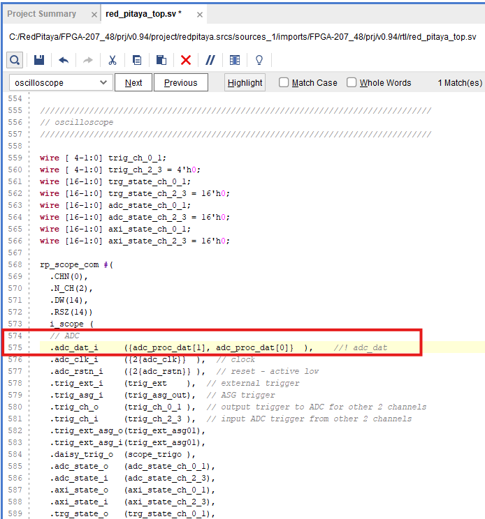
Change the ADC (scope) connections: Change the ADC connections in the oscilloscope (rp_scope_com) component to connect to the new ADC bus instead of the original ADC signals. This will allow us to monitor the processed input signals from our custom component using the oscilloscope application.
// ADC
.adc_dat_i     ({adc_proc_dat[1], adc_proc_dat[0]}  ),    //! adc_dat
Connect the custom component: Finally, we can connect the
adc_dat(adc_dat_swfor SIGNALlab 250-12),asg_datand our two custom busses (adc_proc_datanddac_proc_o) to the custom component.//////////////////////////////////////////////////// // Custom processing component //////////////////////////////////////////////////// red_pitaya_proc #( .DW (DWE ) // GPIO bus width ) i_proc( // Signals .clk_i (adc_clk ), // clock .rstn_i (adc_rstn ), // reset - active low // ADC .adc_a_in (adc_dat[0] ), // IN 1 - ADC input .adc_b_in (adc_dat[1] ), // IN 2 - ADC input .adc_a_out (adc_proc_dat[0] ), // IN 1 - to scope .adc_b_out (adc_proc_dat[1] ), // IN 2 - to scope // DAC .dac_a_in (asg_dat[0] ), // OUT 1 - from signal generator (ASG) .dac_b_in (asg_dat[1] ), // OUT 2 - from signal generator (ASG) .dac_a_out (dac_proc_o[0] ), // OUT 1 - DAC output .dac_b_out (dac_proc_o[1] ), // OUT 2 - DAC output // GPIO + LED .led_o (led_o ), // LED output .gpio_p_in (exp_p_in ), // GPIO P row input .gpio_p_out (exp_p_out ), // GPIO P row output .gpio_p_dir (exp_p_dir ), // GPIO P row direction .gpio_n_in (exp_n_in ), // GPIO N row input .gpio_n_out (exp_n_out ), // GPIO N row output .gpio_n_dir (exp_n_dir ), // GPIO N row direction // System bus .sys_addr (sys[3].addr ), // System address .sys_wdata (sys[3].wdata ), // Write data .sys_wen (sys[3].wen ), // Write enable .sys_ren (sys[3].ren ), // Read enable .sys_rdata (sys[3].rdata ), // Read data .sys_err (sys[3].err ), // Error .sys_ack (sys[3].ack ) // Acknowledge );
Note
Since we disconnected the GPIOs and LEDs from the House Keeping module, SCPI and API commands to control them will not work. It is possible to add custom registers for GPIO and LED control in the custom component (covered in a different tutorial).
The DAC signal from the custom component is summed with the output of the existing signal generator (if enabled). If you want to use only the custom component’s DAC output, you can modify the DAC IO section to remove the signal generator’s contribution or exclude the ASG component from the design.
Confirm unknown component: After we save the changes to the red_pitaya_top.sv file, we will see Vivado add an unknown component to the Design Sources panel. This is because we haven’t created the custom component yet.
Designing a new custom component
Due to the “black box” nature of HDL languages, we can write the custom component in any HDL language (Verilog, VHDL, etc.) and it will work as long as the input and output ports match the expected names, widths, and directions. We will create both a Verilog and a VHDL version of the custom component.
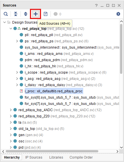
Add a new Design Source: To add a new Design Source to the project, either click the + button in the Sources panel or right-click on the Design Sources directory and select Add Sources.
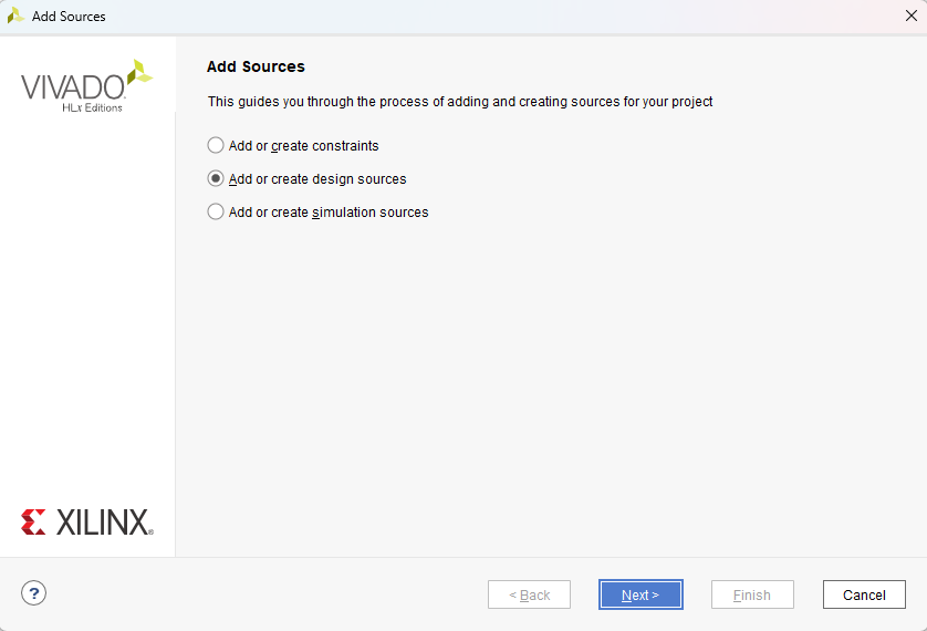
As we are adding a new module, we need to select Add or create design sources.
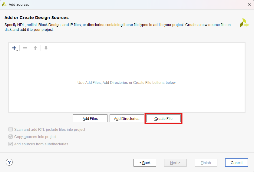
If we already have the HDL code for the custom component, we can select Add Files and browse to the file location. In this case, we will create a new file, so select Create File.
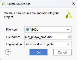
Select the File type: Select the File type (Verilog or VHDL) and enter the File name (red_pitaya_proc). Click OK to create the new file.
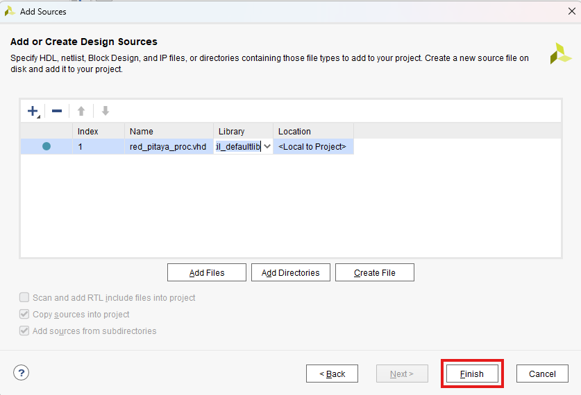
Finish adding the new file: The new file will be added to the list of files to be added to the project. Click Finish to complete the process.
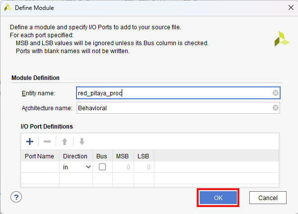
Define the Module: As soon as the file is created, another window will pop up, asking for the Module definition parameters like entity name, architecture name and I/O ports. We will click OK as it is much easier to edit the ports in the code editor directly.
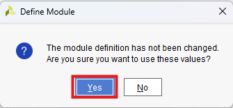
Confirm Module Definition: Click Yes.
Open the new file: After Vivado finishes reloading, we will see the new file in the Design Sources panel. Double-click the file name to open it in the editor.
Copy the code: Now, copy the following code into the file. We will go through its functionality step by step.
library IEEE;
use IEEE.std_logic_1164.all;
use IEEE.numeric_std.all;

entity red_pitaya_proc is
generic(
  DW                      :       integer := 8                        -- GPIO width
);
port (
  clk_i                   : in    std_logic;
  rstn_i                  : in    std_logic;                          -- bus reset - active low

  sys_addr                : in    std_logic_vector(31 downto 0);      -- bus address
  sys_wdata               : in    std_logic_vector(31 downto 0);      -- bus write data
  sys_wen                 : in    std_logic;                          -- bus write enable
  sys_ren                 : in    std_logic;                          -- bus read enable
  sys_rdata               : out   std_logic_vector(31 downto 0);      -- bus read data
  sys_err                 : out   std_logic;                          -- bus error indicator
  sys_ack                 : out   std_logic;                          -- bus acknowledge signal

  adc_a_in, adc_b_in      : in    signed(13 downto 0);                -- ADC 1 & 2 input
  adc_a_out, adc_b_out    : out   signed(13 downto 0);                -- to scope

  dac_a_in, dac_b_in      : in    signed(13 downto 0);                -- from signal generator (ASG)
  dac_a_out, dac_b_out    : out   signed(13 downto 0);                -- DAC 1 & 2 output

  led_o                   : out   std_logic_vector(   7 downto 0);    -- LED output
  gpio_p_in, gpio_n_in    : in    std_logic_vector(DW-1 downto 0);    -- GPIO input data
  gpio_p_out, gpio_n_out  : out   std_logic_vector(DW-1 downto 0);    -- GPIO output data
  gpio_p_dir, gpio_n_dir  : out   std_logic_vector(DW-1 downto 0)     -- GPIO direction
);
end red_pitaya_proc;

architecture RTL of red_pitaya_proc is

-- ### SIGNALS ### --
constant ZERO           : std_logic_vector(31 downto 0) := (others => '0');         -- Padding registers
constant ID_REG         : std_logic_vector(31 downto 0) := X"FEEDBACC";             -- ID register

-- LED & GPIO --

signal diop_in,  dion_in    : std_logic_vector(DW-1 downto 0);                      -- GPIO input
signal diop_out, dion_out   : std_logic_vector(DW-1 downto 0) := (others => '0');   -- GPIO output
signal diop_dir, dion_dir   : std_logic_vector(DW-1 downto 0) := (others => '0');   -- Direction in == 0, out == 1

signal led                  : std_logic_vector(   7 downto 0) := (others => '0');   -- LED status

begin

-- ### Registers, write & control logic ### --
-- Red Pitaya core clock frequency
pbus: process(clk_i)
begin
  if rising_edge(clk_i) then
    if rstn_i = '0' then
      -- LED & GPIO --
      diop_dir <= (others => '0');
      dion_dir <= (others => '0');
      diop_out <= (others => '0');
      dion_out <= (others => '0');
      led <= (others => '0');

    else
      sys_ack <= sys_wen or sys_ren;                      -- acknowledge transactions

      -- decode address & write registers
      if sys_wen='1' then
        if    sys_addr(19 downto 0) = X"00010" then
          diop_dir <= sys_wdata(DW-1 downto 0);           -- Change direction P

        elsif sys_addr(19 downto 0) = X"00014" then
          dion_dir <= sys_wdata(DW-1 downto 0);           -- Change direction N

        elsif sys_addr(19 downto 0) = X"00018" then
          diop_out <= sys_wdata(DW-1 downto 0);           -- Change output P

        elsif sys_addr(19 downto 0) = X"0001C" then
          dion_out <= sys_wdata(DW-1 downto 0);           -- Change output N

        elsif sys_addr(19 downto 0) = X"00030" then
          led <= sys_wdata(7 downto 0);                   -- Change LEDs

        end if;
      end if;
    end if;
  end if;
end process pbus;

sys_err <= '0';

-- ADC & DAC processing --
adc_a_out <= adc_a_in;
adc_b_out <= adc_b_in;
dac_a_out <= dac_a_in;
dac_b_out <= dac_b_in;

-- GPIO I/O assignment --
gpio_p_out <= diop_out;
gpio_n_out <= dion_out;
gpio_p_dir <= diop_dir;
gpio_n_dir <= dion_dir;
diop_in <= gpio_p_in;
dion_in <= gpio_n_in;

-- LED output assignment --
led_o <= led;


-- ### Decode address & read data ### --
with sys_addr(19 downto 0) select
  sys_rdata <=                          ID_REG              when x"00000",      -- ID register
              ZERO(32-1 downto DW)    & diop_dir            when x"00010",      -- GPIO P direction
              ZERO(32-1 downto DW)    & dion_dir            when x"00014",      -- GPIO N direction
              ZERO(32-1 downto DW)    & diop_out            when x"00018",      -- GPIO P output
              ZERO(32-1 downto DW)    & dion_out            when x"0001C",      -- GPIO N output
              ZERO(32-1 downto DW)    & diop_in             when x"00020",      -- GPIO P inputs
              ZERO(32-1 downto DW)    & dion_in             when x"00024",      -- GPIO N inputs
              ZERO(32-1 downto  8)    & led                 when x"00030",      -- LEDs
              ZERO when others;

end RTL;
module red_pitaya_proc # (
  parameter DW = 8                                // Digital width (number of GPIO pins)
) (
  input                clk_i,                     // Clock input
  input                rstn_i,                    // bus reset - active low

  input       [  31:0] sys_addr,                  // bus address
  input       [  31:0] sys_wdata,                 // bus write data
  input                sys_wen,                   // bus write enable
  input                sys_ren,                   // bus read enable
  output reg  [  31:0] sys_rdata,                 // bus read data
  output wire          sys_err,                   // bus error indicator
  output reg           sys_ack,                   // bus acknowledge signal

  input       [  13:0] adc_a_in, adc_b_in,        // ADC 1 & 2 input
  output wire [  13:0] adc_a_out, adc_b_out,      // to scope

  input       [  13:0] dac_a_in, dac_b_in,        // from signal generator (ASG)
  output wire [  13:0] dac_a_out, dac_b_out,      // DAC 1 & 2 output

  output wire [   7:0] led_o,                     // LED output
  input       [DW-1:0] gpio_p_in, gpio_n_in,      // GPIO input data
  output wire [DW-1:0] gpio_p_out, gpio_n_out,    // GPIO output data
  output wire [DW-1:0] gpio_p_dir, gpio_n_dir     // GPIO direction
);

  // Internal signals
  reg        [DW-1:0] diop_dir;
  reg        [DW-1:0] dion_dir;
  reg        [DW-1:0] diop_out;
  reg        [DW-1:0] dion_out;
  wire       [DW-1:0] diop_in;
  wire       [DW-1:0] dion_in;
  reg        [   7:0] led;

  // ADC & DAC passthrough
  assign adc_a_out = adc_a_in;
  assign adc_b_out = adc_b_in;
  assign dac_a_out = dac_a_in;
  assign dac_b_out = dac_b_in;

  // Bus process
  always @(posedge clk_i) begin
    if (!rstn_i) begin
      diop_dir <= {DW{1'b0}};
      dion_dir <= {DW{1'b0}};
      diop_out <= {DW{1'b0}};
      dion_out <= {DW{1'b0}};
      led      <= 8'b0;
    end else begin
      sys_ack <= sys_wen | sys_ren;

      if (sys_wen) begin
        case (sys_addr[19:0])
          20'h00010: diop_dir <= sys_wdata[DW-1:0];
          20'h00014: dion_dir <= sys_wdata[DW-1:0];
          20'h00018: diop_out <= sys_wdata[DW-1:0];
          20'h0001C: dion_out <= sys_wdata[DW-1:0];
          20'h00030: led      <= sys_wdata[7:0];
        endcase
      end
    end
  end

  // Error handling
  assign sys_err = 1'b0;

  // Direct connections
  assign gpio_p_dir = diop_dir;
  assign gpio_n_dir = dion_dir;
  assign gpio_p_out = diop_out;
  assign gpio_n_out = dion_out;
  assign diop_in    = gpio_p_in;
  assign dion_in    = gpio_n_in;
  assign led_o      = led;

  // Read data
  always @(*) begin
    case (sys_addr[19:0])
      20'h00000: sys_rdata = 32'hFEEDBACC;
      20'h00010: sys_rdata = {{32-DW{1'b0}}, diop_dir};
      20'h00014: sys_rdata = {{32-DW{1'b0}}, dion_dir};
      20'h00018: sys_rdata = {{32-DW{1'b0}}, diop_out};
      20'h0001C: sys_rdata = {{32-DW{1'b0}}, dion_out};
      20'h00020: sys_rdata = {{32-DW{1'b0}}, diop_in};
      20'h00024: sys_rdata = {{32-DW{1'b0}}, dion_in};
      20'h00030: sys_rdata = {{32-8{1'b0}},  led};
      default:   sys_rdata = 32'b0;
    endcase
  end
endmodule
The code of the custom component is relatively simple and has the following functionality:
ID register.
LED and GPIO control via the system bus.
Passthrough of ADC and DAC signals (input signals are sent to the scope, output signals are sent to the DAC).
As discussed in v0.94 FPGA project description, the system bus on Red Pitaya is split into eight sections. Each section has its own 20 bit address space.
The custom component is connected to section 3 of the system bus, which has the base address 0x40300000. The upper twelve bits determine the section (0x403 for section 3),
while the lower 20 bits are used for addressing registers inside the component. The custom component has the following registers:
0x00000: ID register0x00010: Digital output direction (diop_dir)0x00014: Digital input direction (dion_dir)0x00018: Digital output data (diop_out)0x0001C: Digital input data (dion_out)0x00030: LED control (led)
The easiest way to interact with the custom FPGA registers from inside Linux OS is through the monitor command line tool.
Save the changes: As soon as we save the changes, Vivado will update the project; our custom module
red_pitaya_procreplaces thered_pitaya_pidmodule, which is now outside the top module.
Proceed with Synthesis, Implementation, and Bitstream Generation as described in the Simple LED blink example above.
In the next chapter we will show how to change the FPGA image on the Red Pitaya board.