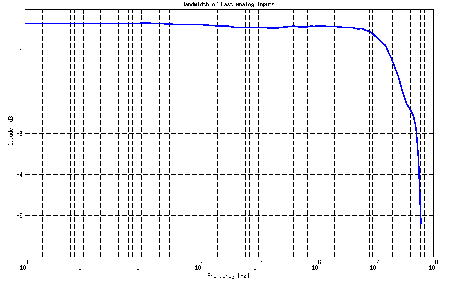
In the picture below, the Frequency Response - Bandwidth of fast analog inputs is shown. Measurements are taken using an Agilent 33250A signal generator as a reference. The measured signal is acquired using remote control commands. An amplitude voltage is extracted from the acquired signal and compared to the reference signal amplitude.
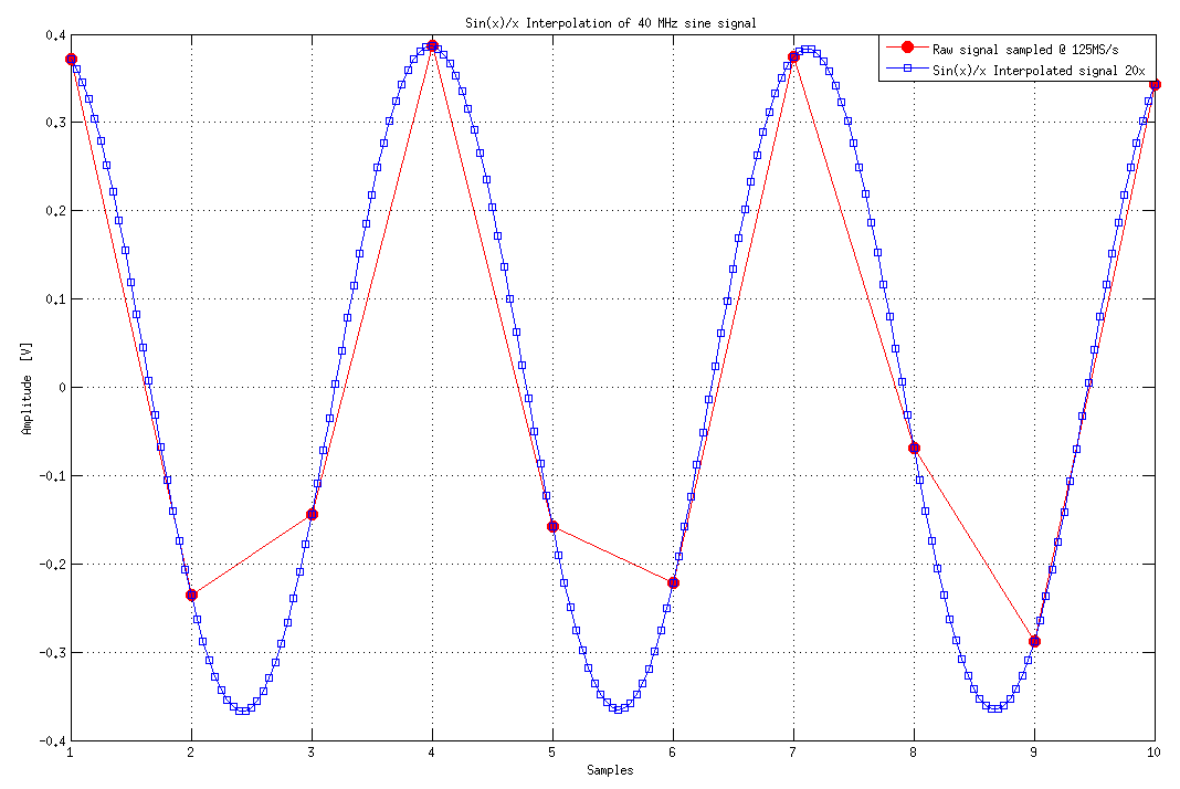
Because of the maximum sampling rate of 125 MS/s when measuring signals above 10 MHz, we have used sin(x)/x interpolation to get more accurate results of Vpp voltage and,
with that, more accurate measurements of analog bandwidth. When measuring signals above 10 MHz, similar results should be obtained without interpolation or directly with an Oscilloscope application and P2P measurements.
Notice: When making measurements without interpolation, you need to extract the maximum and minimum of the acquired signal using a complete 16k buffer.
When using P2P measurements on an oscilloscope, you need to take the maximum value shown as a measurement result. An example of sin(x)/x interpolation for a 40 MHz signal is shown in the picture below (right).
Note
In the picture, only 10 samples of 16k buffer are shown to represent a few periods of 40 MHz signal.
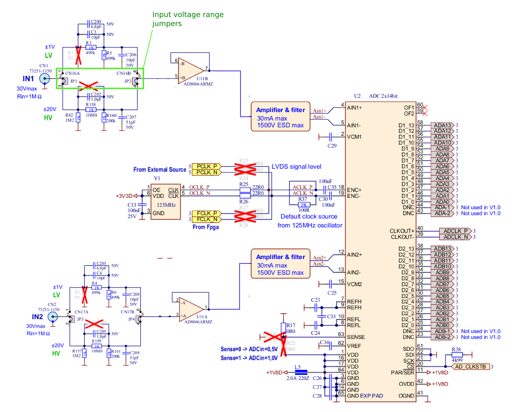
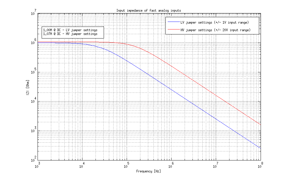
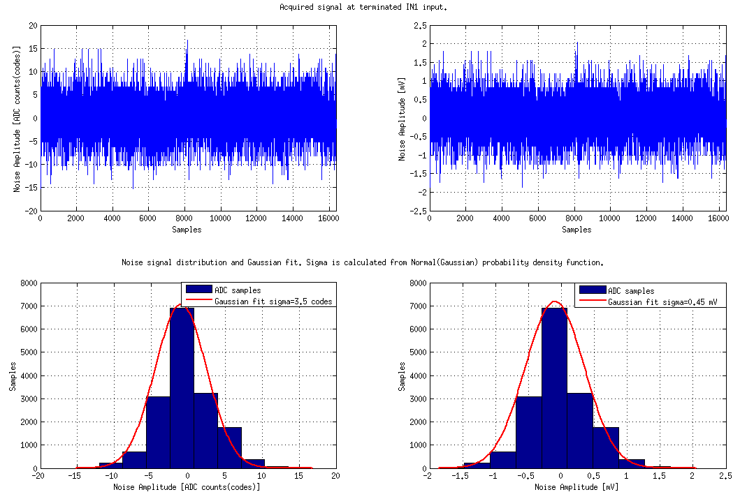
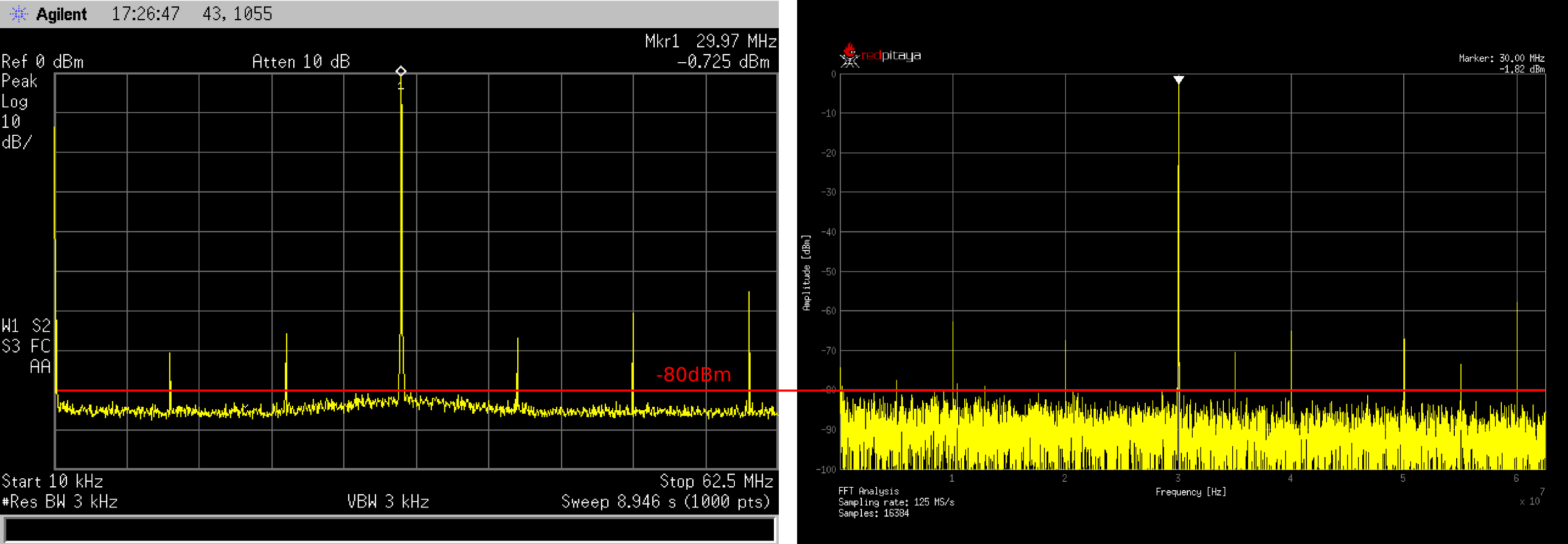
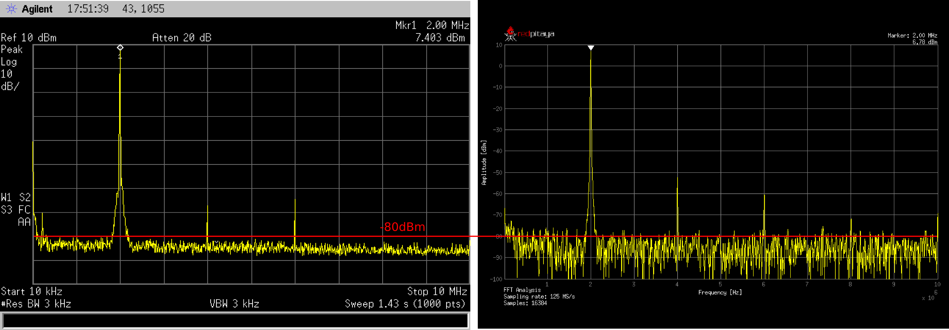
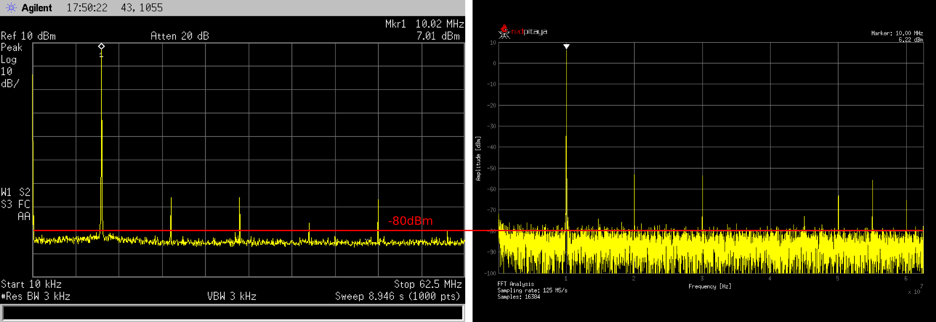
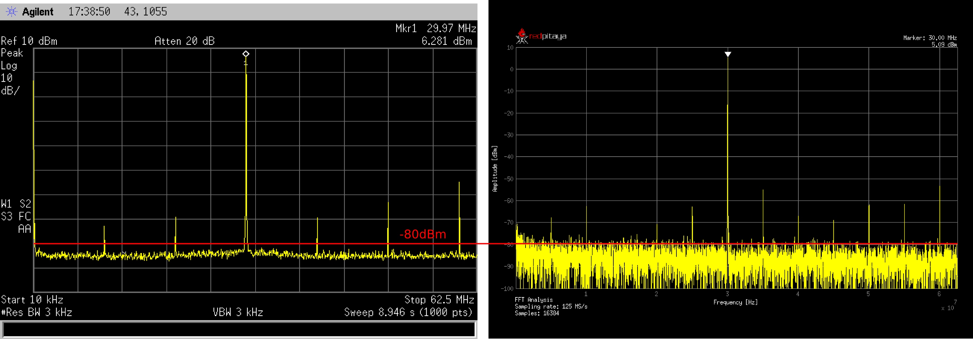
Measurements refer to a high gain (LV ±1 V) jumper setting, with limited environmental noise, inputs and outputs terminated, output signals disabled, and the PCB grounded through SMA ground.
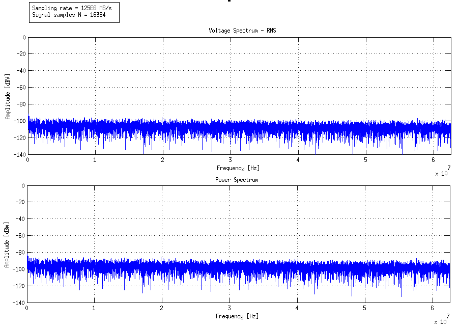
Measurements are performed on 16k continuous samples at full rate (125 MS/s). (Typical full bandwidth std(Vn) < 0.5 mV). The noise spectrum shown in the picture below (right) is calculated using FFT analysis on N = 16384 samples sampled at Fs = 125E6 MS/s.
Crosstalk measurements were performed between input channels 1 and 2 for both LV and HV modes.
Up to 30 MHz
Above 30 MHz
IN1 IN2
LV
HV
LV
HV
LV
>55 dB
>60 dB
40 dB
40 dB
HV
>40 dB
>50 dB
35 dB
35 dB
IN2 IN1
LV
HV
LV
HV
LV
>55 dB
50 dB
40 dB
40 dB
HV
>55 dB
>50 dB
>40 dB
>35 dB
Typical performance:
65 dB @ 10 kHz
50 dB @ 100 kHz
55 dB @ 1 M
55 dB @ 10 MHz
52 dB @ 20 MHz
48 dB @ 30 MHz
44 dB @ 40 MHz
40 dB @ 50 MHz
The typical performance characteristics were measured on LV jumper setting on both channels. The SMA connectors not involved in the measurement are terminated.
The typical measurements refer to the LV jumper setting, inputs matched and outputs terminated, outputs signal disabled, and PCB grounded through SMA ground.
Measurements refer to the LV jumper setting, inputs, and outputs terminated, outputs signal disabled, and the PCB grounded through SMA ground.
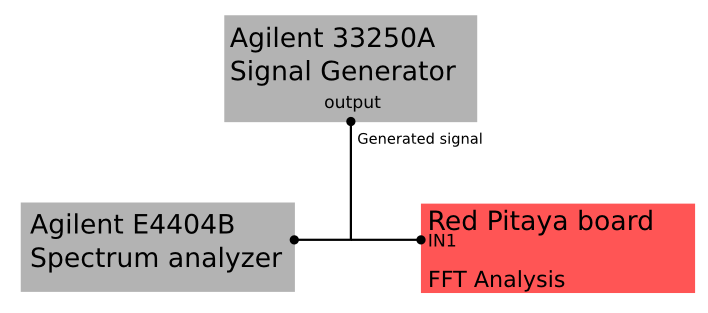
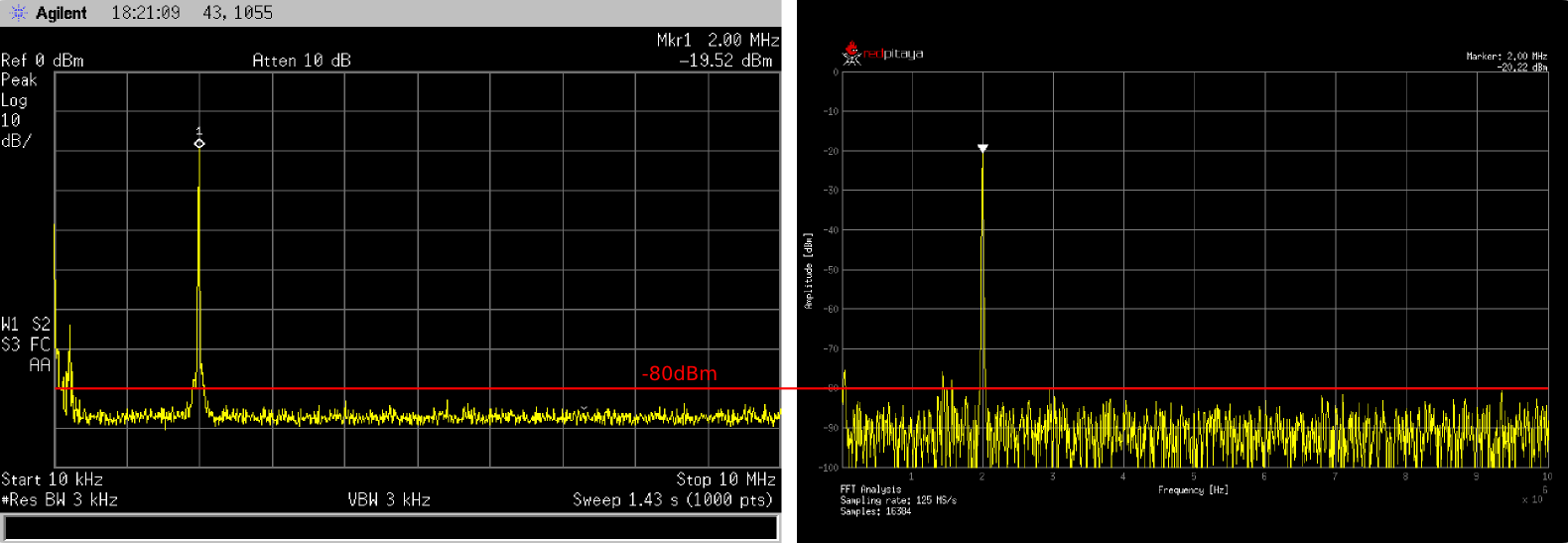
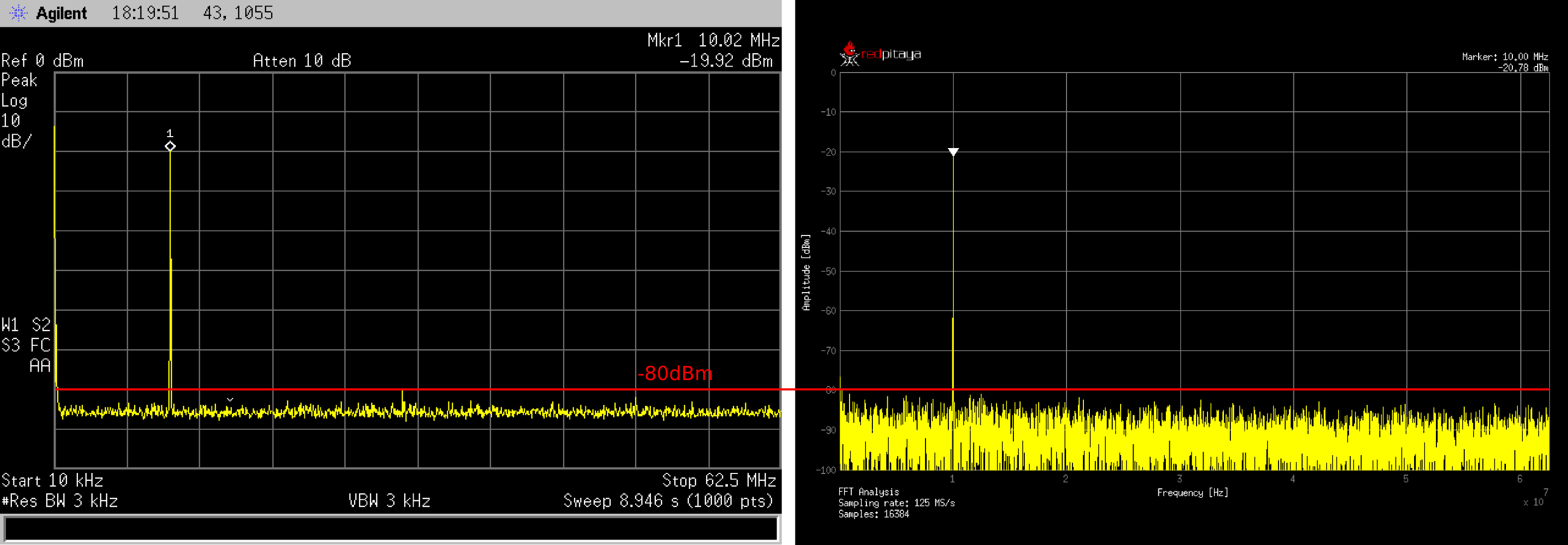
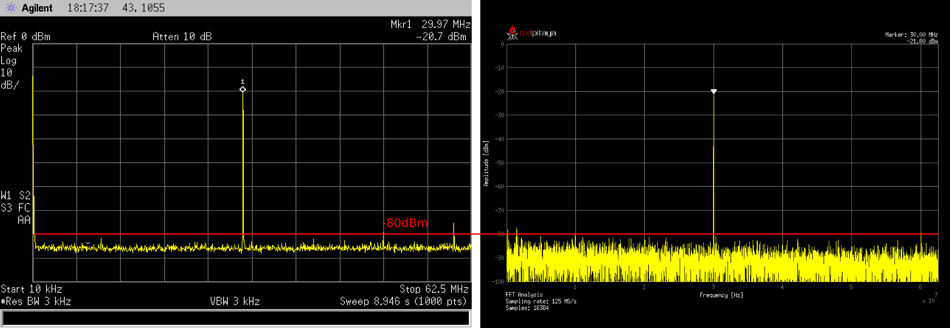
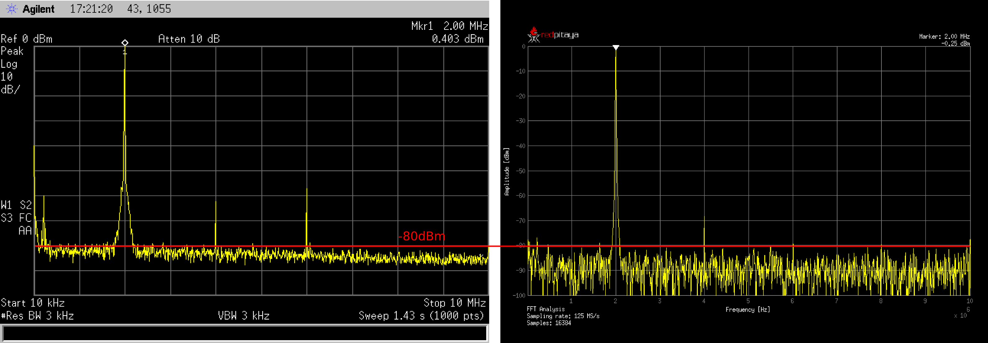
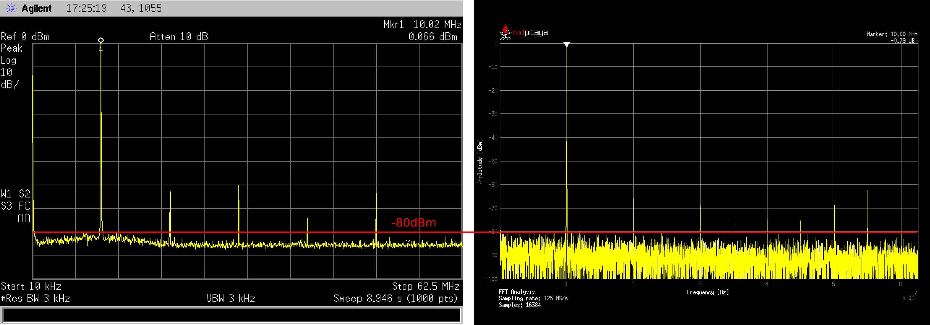
In the pictures below, typical performances of Red Pitaya fast analog inputs are shown. For the reference signal generation, we have used the Agilent 33250A Signal generator.
For the reference spectrum measurements of the generated signal, we have used the Agilent E4404B Spectrum analyzer. The same signal is acquired with the Red Pitaya board and FFT analysis is performed.
Results are shown in the figures below, where Red Pitaya measurements are on the right.
Due to the natural distribution of the electrical characteristics of the analog inputs and outputs, their offsets and gains will differ slightly across various Red Pitaya boards and may change over time. The calibration coefficients are stored in EEPROM on the Red Pitaya and can be accessed and modified with the calibration utility:
root@rp-xxxxxx:~# calib
calib version 2.00-0-f6ded7198Usage: calib [OPTION]...OPTIONS: -r Read calibration values from eeprom (to stdout). The -n flag has no effect. The system automatically determines the type of stored data. -w Write calibration values to eeprom (from stdin). Possible combination of flags: -wn, -wf, -wfn, -wmn, -wfmn -f Use factory address space. -d Reset calibration values in eeprom from factory zone. WARNING: Saves automatic to a new format -i Reset calibration values in eeprom by default Possible combination of flags: -in , -inf. -o Converts the calibration from the user zone to the old calibration format. For ecosystem version 0.98 -v Produce verbose output. -h Print this info. -x Print in hex. -u Print stored calibration in unified format. -m Modify specific parameter in universal calibration -n Flag for working with the new calibration storage format.
The EEPROM is a non-volatile memory, so the calibration coefficients will not change during Red Pitaya power cycles, software upgrades via Bazaar, or manual changes to the contents of the SD card.
An example of reading calibration parameters from the EEPROM with verbose output:
root@rp-xxxxxx:~# calib-r-v
dataStructureId = 5wpCheck = 53count = 28DAC Ch1 Gain (1) = 2674690 # OUT1 gain coefficientDAC Ch1 Offset (2) = -69 # OUT1 DC offsetDAC Ch2 Gain (3) = 2692407 # OUT2 gain coefficientDAC Ch2 Offset (4) = -94 # OUT2 DC offsetADC Ch1 Gain 1/1 (9) = 2817122 # IN1 gain coefficient for LV (±1V range) jumper configurationADC Ch1 Offset 1/1 (10) = -159 # IN1 DC offset for LV (±1V range) jumper configurationADC Ch2 Gain 1/1 (11) = 2811646 # IN2 gain coefficient for LV (±1V range) jumper configurationADC Ch2 Offset 1/1 (12) = -126 # IN2 DC offset for LV (±1V range) jumper configurationADC Ch1 Gain 1/20 (17) = 3113286 # IN1 gain coefficient for HV (±20V range) jumper configurationADC Ch1 Offset 1/20 (18) = -186 # IN1 DC offset for HV (±20V range) jumper configurationADC Ch2 Gain 1/20 (19) = 3115407 # IN2 gain coefficient for HV (±20V range) jumper configurationADC Ch2 Offset 1/20 (20) = -148 # IN2 DC offset for HV (±20V range) jumper configurationADC Ch1 AA 1/1 (33) = 32147 # IN1 FPGA filter coefficient AA for LVADC Ch1 BB 1/1 (34) = 276423 # IN1 FPGA filter coefficient BB for LVADC Ch1 PP 1/1 (35) = 9830 # IN1 FPGA filter coefficient PP for LVADC Ch1 KK 1/1 (36) = 14260634 # IN1 FPGA filter coefficient KK for LVADC Ch2 AA 1/1 (37) = 32147 # IN2 FPGA filter coefficient AA for LVADC Ch2 BB 1/1 (38) = 276423 # IN2 FPGA filter coefficient BB for LVADC Ch2 PP 1/1 (39) = 9830 # IN2 FPGA filter coefficient PP for LVADC Ch2 KK 1/1 (40) = 14260634 # IN2 FPGA filter coefficient KK for LVADC Ch1 AA 1/20 (49) = 16901 # IN1 FPGA filter coefficient AA for HVADC Ch1 BB 1/20 (50) = 193419 # IN1 FPGA filter coefficient BB for HVADC Ch1 PP 1/20 (51) = 9830 # IN1 FPGA filter coefficient PP for HVADC Ch1 KK 1/20 (52) = 14260634 # IN1 FPGA filter coefficient KK for HVADC Ch2 AA 1/20 (53) = 16901 # IN2 FPGA filter coefficient AA for HVADC Ch2 BB 1/20 (54) = 193419 # IN2 FPGA filter coefficient BB for HVADC Ch2 PP 1/20 (55) = 9830 # IN2 FPGA filter coefficient PP for HVADC Ch2 KK 1/20 (56) = 14260634 # IN2 FPGA filter coefficient KK for HV
An example of reading the same calibration parameters from EEPROM with non-verbose output, suitable for editing within scripts:
Should you bring the calibration vector to an undesired state, you can always reset it to factory defaults using the following command:
redpitaya> calib -d
The DC offset calibration parameter can be obtained as the average of the signal acquired with the input grounded.
The calibration parameters can be changed with the Calibration Tool. Alternatively, a reference voltage source and the oscilloscope application can be used to calculate the gain parameter.
Start the oscilloscope application, connect the reference voltage to the desired input and take measurements.
Change the gain calibration parameters as described above, reload the oscilloscope application and take measurements again with the new calibration parameters.
The gain parameters can be optimised by repeating the calibration and measurement steps.
The table below shows typical results after calibration.
Parameter
Jumper settings
Value
DC GAIN ACCURACY @ 122 kS/s
LV
0.2%
DC OFFSET @ 122 kS/s
LV
±0.5 mV
DC GAIN ACCURACY @ 122 kS/s
HV
0.5%
DC OFFSET @ 122 kS/s
HV
±5 mV
AC gain accuracy can be extracted from Frequency response - Bandwidth.