STEMlab 65-16 TI
Overview
The STEMlab 65-16 TI is a premium Red Pitaya board featuring Texas Instruments’ high-performance analog components. With a 16-bit, 62.5 MS/s ADC and ultra-low-jitter clock generator, this board delivers exceptional signal fidelity for precision measurement applications. Built around the AMD Zynq 7020 SoC with 1GB RAM, it combines professional-grade analog performance with powerful FPGA processing.
Features
TI ADC3663 dual-channel 16-bit, 65 MSps SAR ADC with high SNR & low latency
TI DAC2904Y 14-bit, 125 MSps dual-channel DAC with low-jitter outputs
TI LMK03318 ultra-low-jitter clock generator (100 fs RMS @ >100 MHz)
Ultra-low RF output jitter: 5 ps RMS @ 40 MHz (same DAC/clock path as 125-14 TI)
All Gen 2 front-end improvements: improved ENOB, lower noise/jitter
Dual-core ARM Cortex-A9 processor
FPGA AMD (Xilinx) Zynq 7020 SoC
1 GB RAM
22 digital GPIOs, 4 analog inputs, 4 analog outputs
Multiple communication interfaces: I2C, SPI, UART, CAN
USB-C connectivity for power and console
Quick Reference
Category |
Key Specifications |
|---|---|
ADC |
2 channels, 16-bit, 62.5 MS/s, DC-30 MHz |
DAC |
2 channels, 14-bit, 125 MS/s, DC-60 MHz |
Processor |
Dual-core ARM Cortex-A9 |
FPGA |
AMD Zynq 7020 SoC |
RAM |
512 MB |
Digital I/O |
22 GPIOs @ 3.3V |
Analog I/O |
4 inputs (12-bit), 4 outputs (8-bit) |
Jitter Performance |
5 ps RMS @ 40 MHz |
Connectivity |
Ethernet, USB-C, Extension connectors |
Special Features |
High-precision ADC, External ADC clock, PLL |
Board Layout & Pinout

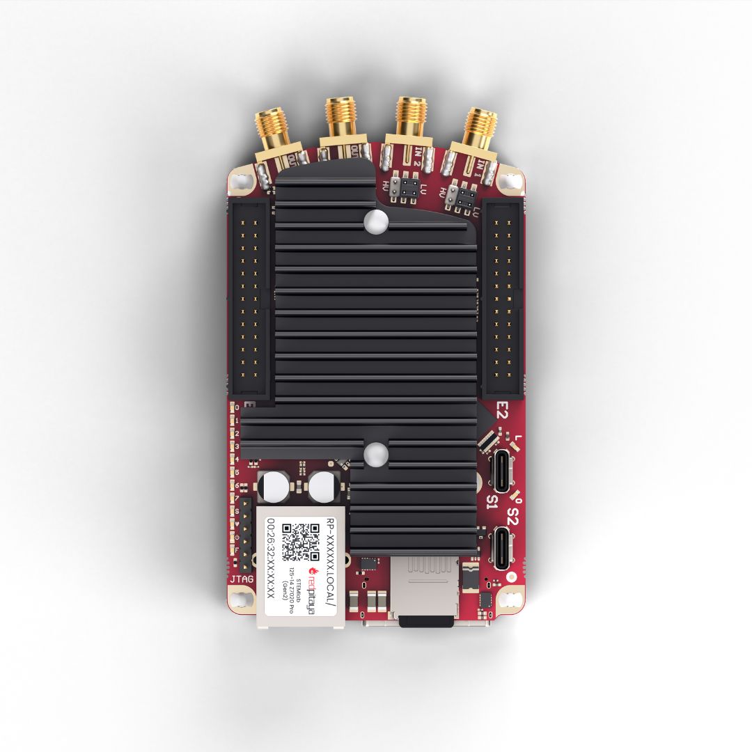
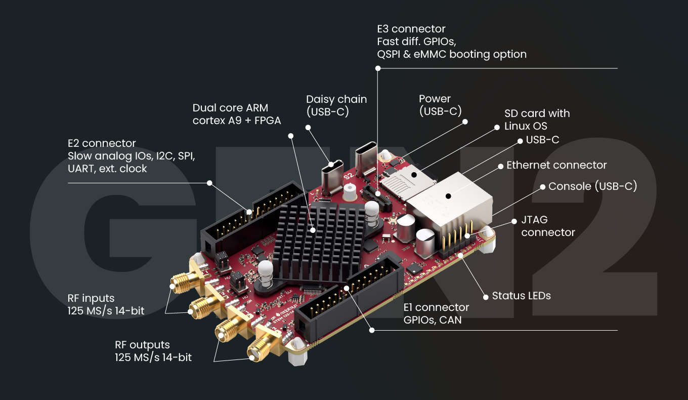
The pinout diagram shows all external connectors including RF inputs/outputs (IN1, IN2, OUT1, OUT2) and extension connectors (E1, E2).
For other external connectors like S1 and S2 synchronisation connectors, power, communication and ethernet ports please see the general Gen 2 picture below.
Technical Specifications
Parameter |
Value |
Units |
Notes |
|---|---|---|---|
|
|||
Processor |
Dual core ARM Cortex-A9 |
- |
|
FPGA |
FPGA AMD (Xilinx) Zynq 7020 SoC |
- |
|
RAM |
512 |
MB |
(4 Gb) |
Core clock frequency |
125 |
MHz |
|
System memory |
Micro SD up to 32 GB |
- |
|
Serial console connector |
USB-C |
- |
|
Power connector |
USB-C |
- |
|
Power consumption |
5 V, 3 A |
- |
Max |
|
|||
Ethernet |
1 |
Gbit |
|
USB |
USB-C 2.0 |
- |
|
Wi-Fi |
Requires Wi-Fi dongle |
- |
|
|
|||
RF input channels |
2 |
- |
|
Sampling rate |
62.5 |
MS/s |
|
ADC resolution |
16 |
bit |
|
Input impedance |
1 MΩ / 10 pF |
- |
|
Full scale voltage range |
±1 (LV)
±20 (HV)
|
V |
|
Input coupling |
DC |
- |
|
Absolute max. input voltage |
±6 (LV)
±30 (HV)
|
V |
DC values [1] |
Input ESD protection |
1500 |
V |
DC |
Overload protection |
Protection diodes |
- |
|
Bandwidth |
DC - 30 |
MHz |
|
Connector type |
SMA |
- |
|
|
|||
RF output channels |
2 |
- |
|
Sampling rate |
125 |
MS/s |
|
DAC resolution |
14 |
bit |
|
Load impedance |
50 Ω / Hi-Z |
- |
|
Voltage range |
±1 @ 50 Ω
±2 @ Hi-Z
|
V |
|
Output coupling |
DC |
- |
|
Short circuit protection |
Yes |
- |
|
Output slew rate |
2 V / 10 ns |
- |
|
RF output jitter @40 MHz |
5 |
ps |
RMS |
Bandwidth |
DC - 60 |
MHz |
|
Connector type |
SMA |
- |
|
|
|||
Digital GPIOs |
22 |
- |
|
Digital voltage levels |
3.3 |
V |
|
High-speed diff. pairs (E3) |
N/A |
- |
|
High-speed diff. pair voltage levels (E3) |
N/A |
- |
|
Analog inputs |
4 |
- |
|
Analog input voltage range |
0 - 7.0 |
V |
|
Analog input resolution |
12 |
bit |
|
Analog input sampling rate |
100 |
kS/s |
|
Analog outputs |
4 |
- |
|
Analog output voltage range |
0 - 1.8 |
V |
|
Analog output resolution |
8 |
bit |
|
Analog output sampling rate |
≲ 3.2 |
MS/s |
|
Analog output bandwidth |
≈ 120 |
kHz |
|
Communication interfaces |
I2C, SPI, UART, CAN |
- |
|
Available voltages |
±5, +3.3 |
V |
|
External ADC clock |
Yes |
- |
|
E3 connector |
N/A |
- |
|
|
|||
External trigger input |
DIO0_P |
- |
E1 connector |
External trigger input impedance |
Hi-Z |
- |
Digital input |
Trigger output |
DIO0_N |
- |
E1 connector [2] |
Daisy chain connectors (S1 & S2) |
Yes |
- |
|
Daisy chain connectors speed |
up to 500 |
Mb/s |
|
Daisy chain connectors type |
USB-C |
- |
Not standard USB-C [3] |
Ref. clock input |
Yes |
- |
Via Ext. ADC Clk± [4] |
Ref. clock frequency |
1 - 300 |
MHz |
Default: 125 MHz |
Ref. clock connector type |
Ext. ADC Clk± |
- |
Pins 23/24 on E2 connector |
|
|||
SD card |
Yes |
- |
|
QSPI |
Not populated |
- |
See Booting options |
eMMC |
N/A |
- |
|
|
|||
Operating Temperature Range |
0 to 55 |
℃ |
With default heatsink |
Operating Humidity Range |
< 90% |
RH |
|
Automatic Shutdown Temperature |
85 |
℃ |
|
|
|||
Size (L x W x H) |
106.8 x 60.0 x 17.9 |
mm |
See Schematics for details |
Warning
Maximum Input Voltage
LV mode: ±6 V absolute maximum
HV mode: ±30 V absolute maximum
Exceeding these values may damage the board permanently.
See also
For more detailed information, please refer to the Gen 2 board comparison table.
Performance & Measurements
Note
We do not have specific measurements for the STEMlab 65-16 TI board yet. Please refer to the Gen 2 measurements for a general idea of performance.
You can find the measurements of the fast analog frontend here:
Schematics & 3D Models
Schematics
Note
Full hardware schematics for the Red Pitaya board are not available. Red Pitaya has open-source code but not open hardware schematics. Nonetheless, development schematics are available. This schematic will give you information about hardware configuration, FPGA pin connections, and similar.
Mechanical Specifications and 3D Models
Note
3D models for the STEMlab 65-16 TI board are not currently available. They will be uploaded in the future.
Hardware Details
Key Components
Signal Path Components
The STEMlab 65-16 TI uses high-performance Texas Instruments components for the signal chain, providing superior performance with 16-bit ADC resolution.
ADC: Texas Instruments ADC3663
Dual 16-bit, 65 MS/s ADC
Ultra-low noise and high linearity
Excellent dynamic range
DAC: Texas Instruments DAC2904
Quad 14-bit, 125 MSPS dual-channel DAC
Low-latency, low-jitter outputs
High SFDR performance
Clock Generator: Texas Instruments LMK03318
Ultra-Low-Noise Jitter Clock Generator
5 ps RMS @ 40 MHz
Programmable frequency synthesis
FPGA: AMD (Xilinx) Zynq 7020
Dual-core ARM Cortex-A9 @ 667 MHz
Programmable logic fabric
Integrated peripherals and memory controllers
Higher logic capacity than Zynq 7010
Oscillator: SG3225VAN
High-precision reference oscillator
Low jitter performance
Supporting Components
Texas Instruments ICs
Protection & Interface:
TPD4E02B04 - ESD protection for USB-C
Logic & Buffers:
SN74AHCT1G125-Q1 - Single buffer/driver with 3-state output
SN74LVC1G86 - Single 2-input XOR gate
Level Translation:
TXS02612 - Voltage level translator
LSF0102 - Bidirectional voltage level translator
PCA9306 - Dual bidirectional I2C bus and SMBus voltage level translator
Power Management:
TPS25821 - USB Type-C and USB Power Delivery controller
TPS62080 - Step-down converter
LM27762 - Dual charge pump plus LDO
Signal Conditioning:
THS4541-Q1 - Differential amplifier
OPA810 - Rail-to-rail operational amplifier
OPA695 - Current feedback operational amplifier
LM393 - Dual comparator
Analog Devices ICs
Power Regulation:
ADP7182 - Linear regulator
ADP151 - Low dropout linear regulator
ADM7170 - Low dropout linear regulator
High-Speed Signal Processing:
AD8007 - High speed op-amp
Extension Connectors & Interfaces
Overview
The STEMlab 65-16 TI board features the following connectors and interfaces:
E1 and E2 connectors: Primary expansion connectors with digital I/O, analog I/O, and communication interfaces. These connectors allow users to interface with additional hardware, sensors, or peripherals, enhancing the board’s capabilities.
S1 and S2 connectors: Daisy-chain connectors for synchronizing multiple Red Pitaya boards. These connectors enable clock and trigger synchronization between boards.
Connector Physical Specifications
E1 and E2 Extension Connectors:
Connector type: 2 x 13 pins IDC 2.54 mm pitch
Pin count: 26 pins each (2x13 configuration)
Pitch: 2.54 mm (0.1”)
Mating Connectors:
Note
When looking for mating connectors for custom Red Pitaya shields, double height elevated sockets are needed to clear the heatsink and ethernet connector on the board. Any connectors with insulation height of 0.635” (16.13 mm) or greater will work. This clearance requirement is based on the tallest components on the Red Pitaya board (heatsink and ethernet connector).
Note
To prevent damage to the board or the shield, when connecting shields to the E1 and E2 connectors, please ensure:
Proper alignment of connectors - ensure the connectors are correctly aligned. The connectors on the Red Pitaya board have additional space in the socket housing, making it possible to misalign the shields by ±1 pin while still appearing physically connected. This can cause damage to the board and/or the shield, so please double-check the alignment before powering on the board.
Tight-fitting counterparts - use connectors that fit securely to prevent accidental disconnections or damage.
E1 Connector - Digital I/O & CAN
The E1 extension connector provides digital I/O and CAN bus interfaces for control and communication applications.
Features:
Two +3V3 power sources (max 0.5 A of current total)
22 single-ended or 11 differential digital I/Os with 3.3 V logic levels
Two CAN buses (configurable via software)
Electrical Specifications:
All DIOx_y pins are LVCMOS33, with the following absolute maximum ratings:
Min. voltage: -0.40 V
Max. voltage: 3.3 V + 0.55 V
Drive strength: < 8 mA
E1 Pinout:
Pin |
Description |
FPGA pin number |
FPGA pin description |
Voltage levels |
|---|---|---|---|---|
1 |
3V3 |
|||
2 |
3V3 |
|||
3 |
DIO0_P / EXT TRIG |
G17 |
IO_L16P_T2_35 |
3V3 |
4 |
DIO0_N / TRIG OUT |
G18 |
IO_L16N_T2_35 |
3V3 |
5 |
DIO1_P |
H16 |
IO_L13P_T2_MRCC_35 |
3V3 |
6 |
DIO1_N |
H17 |
IO_L13N_T2_MRCC_35 |
3V3 |
7 |
DIO2_P |
J18 |
IO_L14P_T2_AD4P_SRCC_35 |
3V3 |
8 |
DIO2_N |
H18 |
IO_L14N_T2_AD4N_SRCC_35 |
3V3 |
9 |
DIO3_P |
K17 |
IO_L12P_T1_MRCC_35 |
3V3 |
10 |
DIO3_N |
K18 |
IO_L12N_T1_MRCC_35 |
3V3 |
11 |
DIO4_P |
L14 |
IO_L22P_T3_AD7P_35 |
3V3 |
12 |
DIO4_N |
L15 |
IO_L22N_T3_AD7N_35 |
3V3 |
13 |
DIO5_P |
L16 |
IO_L11P_T1_SRCC_35 |
3V3 |
14 |
DIO5_N |
L17 |
IO_L11N_T1_SRCC_35 |
3V3 |
15 |
DIO6_P / CAN1_RX |
K16 |
IO_L24P_T3_AD15P_35 |
3V3 |
16 |
DIO6_N / CAN1_TX |
J16 |
IO_L24N_T3_AD15N_35 |
3V3 |
17 |
DIO7_P / CAN0_RX |
M14 |
IO_L23P_T3_35 |
3V3 |
18 |
DIO7_N / CAN0_TX |
M15 |
IO_L23N_T3_35 |
3V3 |
19 |
DIO8_P |
Y9 |
IO_L14P_T2_SRCC_13 |
3V3 |
20 |
DIO8_N |
Y8 |
IO_L14N_T2_SRCC_13 |
3V3 |
21 |
DIO9_P |
Y12 |
IO_L20P_T3_13 |
3V3 |
22 |
DIO9_N |
Y13 |
IO_L20N_T3_13 |
3V3 |
23 |
DIO10_P |
Y7 |
IO_L13P_T2_MRCC_13 |
3V3 |
24 |
DIO10_N |
Y6 |
IO_L13N_T2_MRCC_13 |
3V3 |
25 |
GND |
|||
26 |
GND |
Note
To change the functionality of DIO6_P, DIO6_N, DIO7_P and DIO7_N from GPIO to CAN, please modify the housekeeping register value at address 0x34. For further details, please refer to the FPGA register section.
The change can also be performed with the appropriate SCPI or API command. Please refer to the CAN commands section for further details.
E2 Connector - Analog & Communication
The E2 extension connector provides analog I/O and communication interfaces for sensor integration and data acquisition.
Features:
±5 V power sources (max 0.5 A for +5 V, max 0.1 A for -5 V)
SPI, UART, I2C communication interfaces
4 slow ADCs (12-bit, 100 kS/s)
4 slow DACs (8-bit PWM, ≲ 3.2 MS/s)
External clock input capability
E2 Pinout:
Pin |
Description |
FPGA pin number |
FPGA pin description |
Voltage levels |
|---|---|---|---|---|
1 |
+5V |
|||
2 |
-5V |
|||
3 |
SPI (MOSI) |
E9 |
PS_MIO10_500 |
3V3 |
4 |
SPI (MISO) |
C6 |
PS_MIO11_500 |
3V3 |
5 |
SPI (SCK) |
D9 |
PS_MIO12_500 |
3V3 |
6 |
SPI (CS) |
E8 |
PS_MIO13_500 |
3V3 |
7 |
UART (TX) |
D5 |
PS_MIO8_500 |
3V3 |
8 |
UART (RX) |
B5 |
PS_MIO9_500 |
3V3 |
9 |
I2C (SCL) |
B13 |
PS_MIO50_501 |
3V3 |
10 |
I2C (SDA) |
B9 |
PS_MIO51_501 |
3V3 |
11 |
Ext com. mode (AIN) |
Ext. GND |
||
12 |
GND |
|||
13 |
Analog Input 0 |
B19, A20 |
IO_L2P_T0_AD8P_35, IO_L2N_T0_AD8N_35 |
0-7.0 V |
14 |
Analog Input 1 |
C20, B20 |
IO_L1P_T0_AD0P_35, IO_L1N_T0_AD0N_35 |
0-7.0 V |
15 |
Analog Input 2 |
E17, D18 |
IO_L3P_T0_DQS_AD1P_35, IO_L3N_T0_DQS_AD1N_35 |
0-7.0 V |
16 |
Analog Input 3 |
E18, E19 |
IO_L5P_T0_AD9P_35, IO_L5N_T0_AD9N_35 |
0-7.0 V |
17 |
Analog Output 0 |
T10 |
IO_L1N_T0_34 |
0-1.8 V |
18 |
Analog Output 1 |
T11 |
IO_L1P_T0_34 |
0-1.8 V |
19 |
Analog Output 2 |
P15 |
IO_L24P_T3_34 |
0-1.8 V |
20 |
Analog Output 3 |
U13 |
IO_L3P_T0_DQS_PUDC_B_34 |
0-1.8 V |
21 |
ADC CLK Sel. |
3V3 [5] |
||
22 |
GND |
|||
23 |
Ext. ADC Clk+ [4] |
U18 |
IO_L12P_T1_MRCC_34 |
LVDS [5] |
24 |
Ext. ADC Clk- [4] |
U19 |
IO_L12P_T1_MRCC_34 |
LVDS [5] |
25 |
GND |
|||
26 |
GND |
Auxiliary Analog Inputs & Outputs
Auxiliary Analog Input Channels
The E2 connector provides 4 auxiliary analog inputs for slow-speed measurements and sensor interfacing.
Parameter |
Value |
Units |
Notes |
|---|---|---|---|
Number of channels |
4 |
- |
|
ADC resolution |
12 |
bit |
|
Sampling rate |
100 |
kS/s |
|
Input filter bandwidth |
120 |
kHz |
|
Input voltage range |
0 - 7.0 |
V |
|
Input coupling |
DC |
- |
|
Connector |
Extension connector E2 connector |
- |
Pins 13, 14, 15, 16 |
Auxiliary Analog Output Channels
The E2 connector provides 4 auxiliary analog outputs using PWM with low-pass filtering.
Parameter |
Value |
Units |
Notes |
|---|---|---|---|
Number of channels |
4 |
- |
|
Output resolution |
8 |
bit |
|
Sampling rate |
≲ 3.2 |
MS/s |
|
Output filter bandwidth |
200 |
kHz |
|
Output voltage range |
0 - 1.8 |
V |
|
Output coupling |
DC |
- |
|
Output type |
Low pass filtered PWM |
- |
|
PWM time resolution |
8 ns |
ns |
(1/125 MHz) |
Connector |
Extension connector E2 connector |
- |
Pins 17, 18, 19, 20 |
General Purpose Digital I/O Channels
Parameter |
Value |
Units |
Notes |
|---|---|---|---|
Number of GPIOs |
22 |
- |
|
Digital voltage level |
3.3 |
V |
|
Abs. min. voltage |
-0.40 |
V |
|
Abs. max. voltage |
3.3 + 0.55 |
V |
|
Current limitation |
< 8 |
mA |
Drive strength |
Direction |
Configurable |
- |
|
Time resolution |
8 ns |
ns |
(1/125 MHz) |
Connector location |
Extension connector E1 connector |
- |
Synchronisation Connectors (S1 & S2)
The USB-C S1 and S2 connectors enable daisy chaining of multiple Red Pitaya boards for synchronized multi-channel applications.
S1 Connector (Transmit): Used exclusively for transmitting clock and trigger signals from the current board to the next board in the chain.
S2 Connector (Receive): Used exclusively for receiving clock and trigger signals from the previous board in the chain.
Important
S1 and S2 are NOT standard USB-C ports!
The connectors S1 and S2 are used only for interconnection between Red Pitaya modules. The connection is not compliant with USB-C specification.
Do not connect S1 or S2 to any other USB-C ports except Red Pitaya S1 and S2 connectors (USB ports are DC coupled).
S1 Connector (Transmit)
Pin |
USB-C Signal |
Description |
FPGA pin number |
FPGA pin description |
Voltage levels |
Voltage levels |
FPGA pin description |
FPGA pin number |
Description |
USB-C Signal |
Pin |
|---|---|---|---|---|---|---|---|---|---|---|---|
A1 |
GND |
GND |
B12 |
||||||||
A2 |
TX1+ |
Daisy_IO0_P |
T12 |
IO_L2P_T0_34 |
1V8 |
1V8 |
NC |
RX1+ |
B11 |
||
A3 |
TX1- |
Daisy_IO0_N |
U12 |
IO_L2N_T0_34 |
1V8 |
1V8 |
NC |
RX1- |
B10 |
||
A4 |
VBUS |
VBUS |
B9 |
||||||||
A5 |
CC1 |
S1_Orient [9] |
W6 |
IO_L22N_T3_13 |
3V3 |
3V3 |
NC |
SBU2 |
B8 |
||
A6 |
D1+ |
D2+ |
3V3 |
3V3 |
D1- |
D2- |
B7 |
||||
A7 |
D1- |
D2- |
3V3 |
3V3 |
D1+ |
D2+ |
B6 |
||||
A8 |
SBU1 |
NC |
3V3 |
3V3 |
IO_L22P_T3_13 |
V6 |
S1_Link [9] |
CC2 |
B5 |
||
A9 |
VBUS |
VBUS |
B4 |
||||||||
A10 |
RX2- |
NC |
1V8 |
1V8 |
IO_L11N_T1_SRCC_34 |
U14 |
Daisy_IO1_N |
TX2- |
B3 |
||
A11 |
RX2+ |
NC |
1V8 |
1V8 |
IO_L11P_T1_SRCC_34 |
U15 |
Daisy_IO1_P |
TX2+ |
B2 |
||
A12 |
GND |
GND |
B1 |
S2 Connector (Receive)
Pin |
USB-C Signal |
Description |
FPGA pin number |
FPGA pin description |
Voltage levels |
Voltage levels |
FPGA pin description |
FPGA pin number |
Description |
USB-C Signal |
Pin |
|---|---|---|---|---|---|---|---|---|---|---|---|
A1 |
GND |
GND |
B12 |
||||||||
A2 |
TX1+ |
NC |
1V8 |
1V8 |
Daisy_IO2_P |
RX1+ |
B11 |
||||
A3 |
TX1- |
NC |
1V8 |
1V8 |
Daisy_IO2_N |
RX1- |
B10 |
||||
A4 |
VBUS |
VBUS |
B9 |
||||||||
A5 |
CC1 |
3V3 |
3V3 |
NC |
SBU2 |
B8 |
|||||
A6 |
D1+ |
D2+ |
3V3 |
3V3 |
D1- |
D2- |
B7 |
||||
A7 |
D1- |
D2- |
3V3 |
3V3 |
D1+ |
D2+ |
B6 |
||||
A8 |
SBU1 |
NC |
3V3 |
3V3 |
NC |
CC2 |
B5 |
||||
A9 |
VBUS |
VBUS |
B4 |
||||||||
A10 |
RX2- |
Daisy_IO3_N |
1V8 |
1V8 |
NC |
TX2- |
B3 |
||||
A11 |
RX2+ |
Daisy_IO3_P |
1V8 |
1V8 |
NC |
TX2+ |
B2 |
||||
A12 |
GND |
GND |
B1 |
Advanced Features
Power Supply
Red Pitaya Gen 2 boards support two physical power inputs:
USB-C connector
+5V pin (pin 1) and GND pin (pin 25,26) on the |E2| connector
The sections below describe the supported powering scenarios and their implications.
External Power Specifications:
Parameter |
Specification |
|---|---|
Power supply voltage |
5 V |
Maximum current draw |
3.0 A |
Power supply type |
DC |
Abs. max. voltage |
5.5 V |
Abs. min. voltage |
4.5 V |
Note
The board’s maximum current draw is 3.0 A. The power supply may have a higher current rating — this will not cause any issues.
Note
Why is power protection implemented? The USB-C protection circuit was introduced because boards were being powered from computer USB ports, which typically provide 0.5–0.9 A — insufficient for reliable operation and likely to cause reboots and network disconnections.
Powering scenario 1 — Recommended: USB-C with a standard USB-C power supply
Connect a USB-C power supply (5 V, 3 A) with functional CC lines to the USB-C connector. Leave jumper JP5 unbridged (default).
The USB-C protection circuit detects the CC lines and confirms the supply is USB-C compliant.
The Power Error LED remains off, indicating normal operation.
Full overcurrent protection (3.0 A PTC resettable fuse) is active.
Note
A USB-C power supply without CC lines (e.g. a simple 2-wire USB-C cable with a generic 5 V adapter) will not satisfy the protection circuit and will cause the Power Error LED to light up, as described in scenario 2b below.
Powering scenario 2 — Alternative: 2-pin (non-USB-C) power supply
If a 2-wire 5 V power supply is used (no CC lines), there are two connection options:
2a — Via the E2 connector (+5V pin)
Connect the supply directly to pin 1 (+5V) and pin 25/26 (GND) on the E2 connector connector. The JP5 jumper state does not matter in this case.
The USB-C protection logic is entirely bypassed — the protection circuit is not in the power path.
The 3.0 A PTC resettable fuse on the E2 connector +5V pin remains active for overcurrent protection.
The Power Error LED will be on, because the USB-C protection circuit receives board power but no CC line signal.
2b — Via the USB-C connector
Connect the 2-wire supply through the USB-C connector. JP5 must be bridged to allow power flow in this configuration.
The USB-C protection circuit is in the power path and receives power, but receives no CC line signal.
The Power Error LED will be on — this is expected behaviour, not a fault.
It is the user’s responsibility to verify that the supply provides a stable 5 V at up to 3 A.
Warning
When using scenario 2 (either sub-option), the Power Error LED being on is expected and does not indicate a hardware fault. It indicates that the USB-C protection circuit cannot verify the connected supply’s compliance. The user must ensure the supply meets the 5 V / 3 A specification independently.
Available Power Rails on Extension Connectors:
The E1 connector and E2 connector connector expose several power rails that can be used to supply power to external devices or circuits connected to the board. The current limits below are the maximum currents that Red Pitaya can source from each rail to external loads — they are not related to the board’s own power consumption.
Voltage Rail |
Max. Sourceable Current |
|---|---|
+5 V |
0.5 A [11] |
-5 V |
0.1 A |
+3V3 |
0.5 A [11] |
Note
Exceeding these limits may cause voltage rail instability or trigger the board’s protection circuitry, which can result in a board reset or shutdown.
The +5V pin on E2 connector (pin 1) also serves as a power input when using powering scenario 2a. In that role it is protected by a 3.0 A PTC resettable fuse located on the PCB near the E2 connector connector.
External ADC Clock
Similar to Gen 2 boards, the TI boards also support an external clock input. The main difference, however, is that the TI boards use the LMK03318 Clock Generator, which includes a PLL, frequency synthesizer with integrated VCO, and multiple output drivers instead of just a simple clock switch. The main ADC, DAC, and FPGA CLK signals are all synthesized from the LMK03318 and can differ from each other and the external clock. This means that the external clock supplied through the Ext. ADC Clk± ports on the E2 connector connector can act as a reference for the LMK03318, which in turn generates the main sampling clocks for the ADC, DAC, and FPGA.
By default, the LMK03318 is configured to accept a 125 MHz reference clock, which is then used to generate the 125 MHz sampling clock for the DAC and FPGA, and the 125 MHz or 65 MHz sampling clock for the ADC (depending on the board). If a different external clock frequency is supplied, the LMK03318 must be configured to use that reference frequency instead. |
Clock Selection
Both the internal oscillator clock and the external reference clock signal are connected to the LMK03318 Clock Generator. The CLK_SEL pin (pin 21 on E2 connector) is used to select the reference clock source:
3V3 (logic high) or unconnected: Internal clock (default), supplied from the onboard oscillator.
GND (logic low): External clock, supplied through the Ext. ADC Clk± ports.
Signal Path
The reference clock signal travels to the LMK03318, where it is processed to generate the sampling clocks for the ADC, DAC, and FPGA, and then distributed to these components, ensuring consistent timing across the signal acquisition path.
External Clock Specifications
Parameter |
Description |
Min |
Typ |
Max |
Unit |
|
|---|---|---|---|---|---|---|
Clock input pins |
23 (Clk+) and 24 (Clk-) on E2 connector |
|||||
Input standards |
LVPECL, LVDS, LVCMOS, CML, HCSL |
|||||
Input clock coupling |
AC (on-board capacitors) |
|||||
\(f_{CLK}\) |
Input frequency range |
1 |
125 |
300 |
MHz |
|
\(V_{ID,DIFF,PP}\) |
Input voltage swing |
Differential peak-to-peak |
0.2 |
2.0 |
V |
|
\(\frac{dV}{dt}\) |
Input edge slew rate (20% to 80%) |
Differential, peak-to-peak |
0.5 |
V/ns |
||
Single-ended, non-driven input tied to GND |
0.5 |
V/ns |
||||
IDC |
Input clock duty cycle |
40% |
60% |
|||
Note
The board includes AC coupling capacitors on the external clock inputs, so the input signal must have sufficient amplitude and slew rate to meet the LMK03318 input specifications after AC coupling.
For further information on voltage levels and timing requirements, please refer to the LMK03318 datasheet.
Configuring the external clock frequency
The default LMK03318 configuration is set for a 125 MHz reference clock. If you want to use a different external clock frequency, you need to reconfigure the LMK03318 registers accordingly. This can be done through the I2C interface using the Red Pitaya’s PS side (ARM/Linux). The LMK03318 is available at I2C bus address 0b1010000 (0x50).
To change the reference frequency, you need to calculate the appropriate register settings for the desired frequency and write them to the LMK03318 over I2C.
Note
It is possible to switch the control of the I2C bus to the FPGA (PL side) and implement the I2C interface in the FPGA itself, but this is not supported in the standard Red Pitaya firmware and requires custom FPGA development.
Warning
Changing the external clock frequency during operation is not supported.
The Zynq 7010/7020 PL uses Mixed-Mode Clock Managers (MMCMs) and PLLs to derive internal fabric clocks from the input clock. Changing the external clock frequency during operation will cause the MMCM/PLL to lose lock, resulting in undefined output clocks and acquisition/generation errors. A full FPGA reset or reconfiguration is required after any clock frequency change.
Note
Operating at non-standard clock frequencies:
The Red Pitaya FPGA is designed, tested, and guaranteed to operate correctly at the board’s specified core clock frequency. While it is possible to run the board at different clock frequencies, please be aware that:
FPGA functionality: The official FPGA configuration may not function as intended at non-standard frequencies and requires thorough testing
Sampling rates: The ADC and DAC sampling rates will change proportionally with the clock frequency
Analog bandwidth: The analog bandwidth of the board will change with the clock frequency
Absence of external clock:
OS 2.07-48 or higher: If no valid external clock is present, the PS side will boot using an internal 33 MHz oscillator, but the FPGA will not operate (no signal acquisition/generation functionality)
OS versions prior to 2.07-48: The board will fail to boot (stuck in reboot cycle) if no valid external clock is detected
Note
Advanced: Dynamic clock reconfiguration
The standard Red Pitaya FPGA bitstream does not implement the Dynamic Reconfiguration Port (DRP) interface that AMD (Xilinx) provides for runtime MMCM/PLL reconfiguration. A custom FPGA design using DRP-based MMCM reconfiguration with active lock monitoring could theoretically support runtime clock frequency changes, but this requires extensive FPGA development and verification. The PS side (ARM/Linux) is not affected by clock changes, as it runs from its own independent 33 MHz crystal-derived PLL.
Note
When synchronising multiple Red Pitaya boards, please keep in mind that:
X-channel 2.0 synchronisation (Click Shields) works out-of-the-box
X-channel synchronisation requires a hardware modification as secondary boards differ from the primary board
Booting options
STEMlab 65-16 TI supports QSPI booting, but the QSPI chip is not populated by default. For further information on board modifications, please contact support@redpitaya.com or info@redpitaya.com.
Warning
Any non-Red Pitaya hardware modification will void the warranty, and we cannot guarantee support for modified boards.
Calibration
Red Pitaya Gen 2 boards are factory-calibrated. Recalibration may be required after extended use, environmental changes, or when measurement accuracy degrades.
There are three ways to calibrate the board:
Calibration application — graphical interface accessible from the System Tools menu. Recommended for most users.
Calibration command line utility (calib) — command line tool for scripted or advanced calibration workflows.
C++ or Python API commands — programmatic access to calibration parameters.
For a full description of the calibration procedure, required equipment, and technical reference, please refer to the Calibration documentation.
Note
Gen 2 boards do not require 50 Ω terminators during calibration, unlike the original generation boards. The improved analog front-end circuitry eliminates this requirement.
Additional Resources
For additional specifications and measurements, please refer to:
Gen 2 hardware specifications - Common Gen 2 specifications
Gen 2 board comparison table - Comparison across all Red Pitaya Gen 2 models
Legal & Disclaimers
Note
The information provided by Red Pitaya d.o.o. is believed to be accurate and reliable. However, no liability is accepted for its use. Please note that the contents may be subject to change without prior notice.
Footnotes