Signal Mapping
This section describes the physical connections between Red Pitaya’s FPGA pins and external connectors, including XADC analog inputs, GPIO pins, and LEDs. These mappings are defined in the device tree and are essential for understanding how to interface with Red Pitaya hardware.
See also
For information about device tree configuration and loading, see Device Tree.
XADC Analog Inputs
Red Pitaya provides four analog inputs (AI0-AI3) mapped through the XADC (Xilinx Analog-to-Digital Converter). These inputs are accessible via the Linux IIO (Industrial I/O) subsystem.
Physical Connections
E2 |
ZYNQ p/n |
XADC in |
IIO filename |
Measurement target |
Full scale range |
|---|---|---|---|---|---|
AI0 |
B19/A20 |
AD8 |
in_voltage11_raw |
general purpose |
7.00 V |
AI1 |
C20/B20 |
AD0 |
in_voltage9_raw |
general purpose |
7.00 V |
AI2 |
E17/D18 |
AD1 |
in_voltage10_raw |
general purpose |
7.00 V |
AI3 |
E18/E19 |
AD9 |
in_voltage12_raw |
general purpose |
7.00 V |
K9 /L10 |
AD |
in_voltage8_vpvn_raw |
5V power supply |
6.10 V |
The input range is 0 - 7.0 V by default (unipolar mode).
Bipolar Mode Configuration
For bipolar operation (±3.5 V), resistor R255 must be removed, and Ext. com. mode pin must be connected to a 0.5-1 V voltage reference.
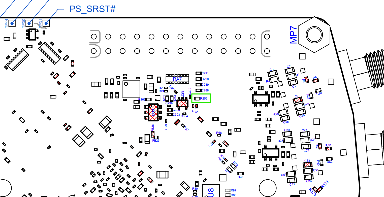
Afterwards, open the Red Pitaya v0.94 (or v0.94_250 for SIGNALlab 250-12) FPGA project. In the block diagram, the XADC wizard has a setting in the Channel Sequencer page to switch the XADCs to bipolar mode. After rebuilding the FPGA, the values are read as 12-bit 2’s complement values.
For bipolar operation (±3.5 V), resistor R273 must be removed, and Ext. com. mode pin must be connected to a 0.5-1 V voltage reference.
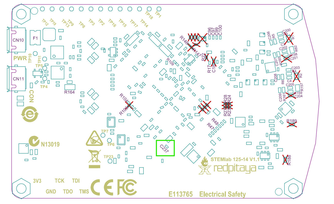
Afterwards, open the Red Pitaya v0.94 (or v0.94_250 for SIGNALlab 250-12) FPGA project. In the block diagram, the XADC wizard has a setting in the Channel Sequencer page to switch the XADCs to bipolar mode. After rebuilding the FPGA, the values are read as 12-bit 2’s complement values.
Voltage Dividers
The XADC inputs use voltage dividers to scale input voltages to the safe range for the ADC.
5V Power Supply
The fourth XADC input (AD) is connected to a voltage divider for measuring the internal 5V power supply voltage:
                       +-----------------0  Vout
          -----------  |  -----------
Vin  0----| 56.0 kΩ |--+--| 4.99 kΩ |----0  GND
          -----------     -----------
Slow Analog Inputs
The XADC auxiliary inputs connected to the slow analog inputs operate in unipolar mode with an input voltage range of 0-1 V. Resistor dividers are used to scale the external input voltage range to 0-7.0 V:
                       +-----------------0  Vout
          -----------  |  -----------
Vin  0----| 30.0 kΩ |--+--| 4.99 kΩ |----0  GND
          -----------     -----------
See also
The voltage dividers were originally designed for a 0-3.5 V range based on an incorrect assumption about the XADC unipolar input range. For the full background, see Slow Analog Input Voltage Range (Original Generation boards) and Slow Analog Input Voltage Range (Gen 2 boards).
Reading XADC Values
XADC values can be read from Linux userspace through the IIO interface:
# Read raw ADC value
cat /sys/bus/iio/devices/iio:device0/in_voltage9_raw

# Read voltage scale
cat /sys/bus/iio/devices/iio:device0/in_voltage9_scale

# Calculate actual voltage: raw_value * scale
Note
The scale factor converts raw ADC readings to millivolts. Remember to account for the voltage divider ratios when calculating actual input voltages.
GPIO and LEDs
Red Pitaya’s GPIO pins and LEDs can be controlled from Linux userspace via sysfs. The handling depends on whether the pins are connected to the PS
(Processing System) or the PL (Programmable Logic). The device tree defines which pins are managed by the PS and which are in the PL.
MIO vs PL/EMIO
MIO (Multiplexed I/O): Pins directly controlled by PS, accessed via standard GPIO
sysfsinterface. Each pin has a few multiplexed functions selectable via pinctrl overlays. The drivers for Linux are provided by AMD/Xilinx.PL/EMIO: Pins controlled by FPGA logic, require FPGA design to define access method (e.g., custom AXI GPIO peripheral). Access method depends on FPGA implementation. If the pin signals in the FPGA sources are wired to EMIO, they can be accessed via the PS GPIO interface.
Warning
The LEDs and GPIOs directly connected to the PS are accessible only if the FPGA is not loaded or if the FPGA code does not change the signal state. Be aware that changing these signals when the FPGA is loaded can cause unpredictable behavior.
GPIO Pin Assignment
The following tables show the complete GPIO pin mapping for Red Pitaya.
PL/EMIO Pins
FPGA |
Connector |
GPIO |
MIO/EMIO index |
|
Comments, LED color, dedicated meaning |
|---|---|---|---|---|---|
Green = Power Good status |
|||||
Blue = FPGA programming DONE |
|||||
|
E1 |
|
|
|
DIO7_N |
|
E1 |
|
|
|
DIO6_N |
|
E1 |
|
|
|
DIO5_N |
|
E1 |
|
|
|
DIO4_N |
|
E1 |
|
|
|
DIO3_N |
|
E1 |
|
|
|
DIO2_N |
|
E1 |
|
|
|
DIO1_N |
|
E1 |
|
|
|
DIO0_N |
|
E1 |
|
|
|
DIO7_P |
|
E1 |
|
|
|
DIO6_P |
|
E1 |
|
|
|
DIO5_P |
|
E1 |
|
|
|
DIO4_P |
|
E1 |
|
|
|
DIO3_P |
|
E1 |
|
|
|
DIO2_P |
|
E1 |
|
|
|
DIO1_P |
|
E1 |
|
|
|
DIO0_P |
|
LED |
|
|
Orange LED7 |
|
|
LED |
|
|
Orange LED6 |
|
|
LED |
|
|
Orange LED5 |
|
|
LED |
|
|
Orange LED4 |
|
|
LED |
|
|
Orange LED3 |
|
|
LED |
|
|
Orange LED2 |
|
|
LED |
|
|
Orange LED1 |
|
|
LED |
|
|
Orange LED0 |
PS MIO Pins
FPGA |
Connector |
GPIO |
MIO/EMIO index |
|
Comments, LED color, dedicated meaning |
|---|---|---|---|---|---|
LED |
|
|
Orange = SD card access |
||
LED |
|
|
Red = CPU heartbeat |
||
|
|
UART1_TX |
|
|
Output only |
|
|
UART1_RX |
|
|
|
|
|
SPI1_MOSI |
|
|
|
|
|
SPI1_MISO |
|
|
|
|
|
SPI1_SCK |
|
|
|
|
|
SPI1_CS# |
|
|
|
|
|
I2C0_SCL |
|
|
|
|
|
I2C0_SDA |
|
|
Linux Sysfs Access
LEDs can be controlled from Linux userspace using the sysfs interface:
# Enable LED heartbeat trigger
echo heartbeat > /sys/class/leds/led0/trigger

# Set LED brightness (0 = off, 1 = on)
echo 1 > /sys/class/leds/led0/brightness

# Turn off LED
echo 0 > /sys/class/leds/led0/brightness
For GPIO pins, use the GPIO sysfs interface:
# Export GPIO pin
echo 960 > /sys/class/gpio/export

# Set direction (out or in)
echo out > /sys/class/gpio/gpio960/direction

# Set value (0 or 1)
echo 1 > /sys/class/gpio/gpio960/value

# Read value
cat /sys/class/gpio/gpio960/value

# Unexport when done
echo 960 > /sys/class/gpio/unexport
PS Pinctrl Overlays
Red Pitaya provides device tree overlay files that allow you to repurpose PS MIO signals. These overlays modify the pinctrl configuration to reassign pins from their default functions (SPI, I2C, UART) to GPIO.
Available Overlays
Overlay File |
Description |
|---|---|
spi2gpio.dtsi |
Reassigns SPI1 signals to GPIO (MOSI, MISO, SCLK, CS) |
i2c2gpio.dtsi |
Reassigns I2C0 signals to GPIO (SDA, SCL) |
uart2gpio.dtsi |
Reassigns UART1 signals to GPIO (TX, RX) |
miso2gpio.dtsi |
Reassigns only MISO signal to GPIO (keeps other SPI1 pins) |
These overlay files are typically included in the project’s device tree source when specific signal configurations are needed.
SPI Configuration Example
The SPI interface on Red Pitaya can be configured through the device tree. A common example is changing the CS (Chip Select) polarity.
By default, the CS state is HIGH (inactive) on all Red Pitaya boards. To set the default value to LOW (active), modify the device tree:
Open the device tree source file:
root@rp-f01c3d:~# rw
root@rp-f01c3d:~# nano /opt/redpitaya/dts/$(monitor -f)/dtraw.dts
Find the SPI device node
spidev@0and add thespi-cs-highproperty:spidev@0 { compatible = "spidev"; reg = <0>; spi-max-frequency = <50000000>; spi-cs-high; /* Add this line */ };
Recompile and reboot:
root@rp-f01c3d:~# cd /opt/redpitaya/dts/$(monitor -f)/
root@rp-f01c3d:~# dtc -I dts -O dtb ./dtraw.dts -o devicetree.dtb
root@rp-f01c3d:~# reboot
Note
The settings are applied only after the device tree is loaded. When the board starts up, the CS value is in the HIGH state but will change to LOW after the boot is complete.
Note
You can also switch the SPI CS mode at runtime through the Red Pitaya API:
rp_SPI_GetCSModerp_SPI_SetCSMode
See the hw api command reference for more details.
Troubleshooting
GPIO/LED Access Issues
Error: Permission denied when accessing sysfs
Cause: Insufficient permissions or SELinux restrictions
Solution:
Run commands as root or use sudo
Check file permissions in /sys/class/gpio/ or /sys/class/leds/
Error: GPIO already exported
Cause: GPIO pin already exported by another process or previous session
Solution:
Unexport the GPIO:
echo <pin_number> > /sys/class/gpio/unexportCheck for other processes using the GPIO:
lsof | grep gpio
Symptom: GPIO changes don’t affect hardware
Cause: FPGA is loaded and controlling the pins
Solution:
Unload FPGA or use FPGA that doesn’t control these pins
Use appropriate MIO pins instead of EMIO pins if PS control is needed
XADC Reading Issues
Error: IIO device not found
Cause: XADC not enabled in device tree or driver not loaded
Solution:
Verify xadc node exists in device tree
Check if IIO driver is loaded:
lsmod | grep xilinxVerify device appears in /sys/bus/iio/devices/
Symptom: Incorrect voltage readings
Cause: Wrong scaling factor or voltage divider calculation
Solution:
Verify using correct formula for input type (5V supply vs general purpose)
Check if bipolar mode resistor R273 (original) or R255 (Gen 2) is present/removed as expected
Calibrate readings against known reference voltage
Additional Resources
Device Tree - Device tree configuration and compilation
Installation of Xilinx SDK 2019.1 - SDK installation and HSI tool usage
Overlay Utility (FPGA Configuration) - Quick reference for overlay script
Advanced FPGA Loading - Comprehensive overlay script guide
Linux IIO Documentation - Industrial I/O subsystem documentation
GPIO Sysfs Interface - Kernel GPIO interface documentation