3.2.2.3. Build FPGA image
Index
The following build instructions were tested on Ubuntu 20.04. It is important to install the correct Vivado and SDK versions as the projects and scripts are made for those versions and may return errors during the build.
Note
Please note that the FPGA code is located in a separate repository from the ecosystem on our GitHub page:
Ecosystem: RedPitaya/RedPitaya
FPGA: RedPitaya/RedPitaya-FPGA
Running the “Makefile.x86” will download the necessary files from the RedPitaya/RedPitaya-FPGA repository.
For building the FPGA image for different boards please see the Buildprocess.
3.2.2.3.1. Prerequisites
3.2.2.3.1.1. Libraries used by ModelSim-Altera
Install libraries:
# apt-get install unixodbc unixodbc-dev libncurses-dev libzmq3-dev libxext6 libasound2 libxml2 libx11-6 libxtst6 libedit-dev libxft-dev libxi6 libx11-6:i386 libxau6:i386 libxdmcp6:i386 libxext6:i386 libxft-dev:i386 libxrender-dev:i386 libxt6:i386 libxtst6:i386
3.2.2.3.1.2. Xilinx Vivado 2020.1
Xilinx Vivado is available from the Xilinx downloads page.
Note
Please note that it might be necessary to download the Full installer as the Web installer might give an Installer outdated warning and refuse to proceed with the installation process.
Additionally, on officially unsupported versions of Linux, the installer gives you a warning, but Vivado should work fine, for example running it on Ubuntu 20.04 or 22.04 instead of 18.04.
If the installer glitches out anyway, your /etc/os-release file needs to be changed to “fake” the OS version. First, backup the file and then open it as a superuser with a text editor such as nano:
$ sudo nano /etc/os-release
and change the VERSION line to VERSION=”18.04.4 LTS (Bionic Beaver)" and save the file. The edited file should look something like this:
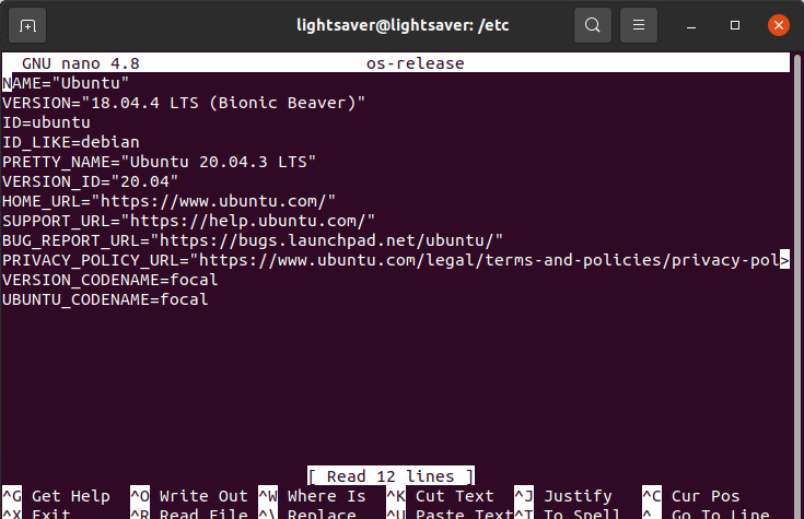
Afterward, you can either run the Xilinx_Unified_2020.1_0602_1208_Lin64.bin (Linux web installer) or the xsetup file from the extracted folder (unified installer). After the installation finishes replace the modified file with the one you backed up – failure to do so might cause some problems with other programs.
For more information on Vivado installation click here.
3.2.2.3.1.3. Xilinx SDK development environments 2019.1
Note
Please note that it might be necessary to download the Full installer as the Web installer might give an Installer outdated warning and refuse to proceed with the installation process.
Xilinx SDK is available from the Xilinx downloads page.
3.2.2.3.1.4. Device Tree Xilinx
FPGA build requires a repository with a device tree from Xilinx. You can prepare it by running the command:
$ make -f Makefile.x86 devicetree
Note
The file can be manually uploaded.
curl -L https://github.com/Xilinx/device-tree-xlnx/archive/xilinx-v2017.2.tar.gz/ -o device-tree-xlnx-xilinx-v2017.2.tar.gz
Extract the .tar.gz to /<redpitaya path>/tmp/device-tree-xlnx-xilinx-v2017.2.
3.2.2.3.2. Directory structure
There are multiple FPGA projects, some with generic functionality, some with specific functionality for an application.
Common code for all projects is placed directly into the FPGA directory. Common codes are mostly reusable modules.
Project-specific code is placed inside the fpga/prj/name/ directories and is similarly organized as common code.
path |
contents |
|---|---|
|
main Makefile, used to run FPGA-related tools |
|
TCL scripts to be run inside FPGA tools |
|
archive of XZ compressed FPGA bit files |
|
documentation (block diagrams, address space, …) |
|
board files Vivado System-Level Design Entry |
|
third party IP, for now, Zynq block diagrams |
|
Verilog (SystemVerilog) Register-Transfer Level |
|
Synopsys Design Constraints contains Xilinx design constraints |
|
simulation scripts |
|
Verilog (SystemVerilog) test bench |
|
device tree source include files |
|
project name specific code |
|
Hardware Software Interface contains FSBL (First Stage Boot Loader) and DTS (Design Tree) builds |
3.2.2.3.3. FPGA sub-projects
There are multiple FPGA sub-projects they mostly contain incremental changes on the first Red Pitaya release.
Note
If unsure which FPGA project to use for you project, please look at the “Application” column, where examples of use are presented.
It is recommended to use the 0.94 release as the default project.
prj/name |
Description |
Application |
|---|---|---|
0.93 |
This is the original Red Pitaya release including all bugs. For deprecated application backward compatibility only. |
|
0.94 |
|
Oscilloscope |
stream_app |
|
Streaming manager |
classic |
|
|
logic |
This image is used by the logic analyzer, it is using DMA to |
Logic analyzer |
axi4lite |
Image intended for testing various AXI4 bus implementations. |
3.2.2.3.4. Building process
The following table shows which projects are available on which boards.
Build name |
Build Project Flag |
STEMlab 125-10 |
SIGNALlab 250-12 |
SDRlab 122-16 |
STEMlab 125-14 4-Input |
|---|---|---|---|---|---|
0.94 |
v0.94 |
X |
X |
X |
|
0.94_250 |
v0.94_250 |
X |
|||
stream_app |
stream_app |
X |
X |
||
stream_app_250 |
stream_app_250 |
X |
|||
logic |
logic |
X |
|||
logic_250 |
logic_250 |
X |
|||
tft |
tft |
X |
|||
axi4lite |
axi4lite |
X |
|||
classic |
classic |
X |
|||
mercury |
mercury |
X |
Table of required build flags for FPGA projects per board
Model |
Build Model flag |
|---|---|
STEMlab 125-10 |
MODEL=Z10 |
STEMlab 125-14-Z7020 |
MODEL=Z20_14 |
SDRlab 122-16 |
MODEL=Z20 |
SIGNALlab 250-12 |
MODEL=Z20_250 |
STEMlab 125-14 4-Input |
MODEL=Z20_125_4CH |
On the PC that has Vivado installed run the following commands to properly configure system variables (needs to be done every time you open a new terminal window). Alternatively, you can add the following lines to your .bashrc file using a text editor – this will ensure that they are run at the system startup:
source <path to Xilinx installation directory>/Xilinx/Vivado/2020.1/settings64.sh
source <path to Xilinx installation directory>/Xilinx/SDK/2019.1/settings64.sh
The Xilinx installation directory should be located in /opt directory (or /tools, if you used the default Vivado installation directory). These two commands will set up the $PATH environment variable. It might also be necessary to add the SDK bin folder to the $PATH environment variable:
export PATH=<path to Xilinx installation directory>/Xilinx/SDK/2019.1/bin:$PATHOn Windows, please check this link or search the web. Add the path to the /bin directory for Vivado and SDK.
Check if you have Git command line tools installed on your computer:
sudo apt update
sudo apt install git
Create a new directory for the Red Pitaya code. Then download the code by running the following command in the newly created directory:
git clone https://github.com/RedPitaya/RedPitaya.gitNote
For an alternative way to create an FPGA project plese check Red Pitaya FPGA tutorial. If following the FPGA tutorial you can reffer to step 6 and later in this section, please note that all paths in the following section start with <Red Pitaya repository>/RedPitaya-FPGA/prj instead of <Red Pitaya repository>/fpga/prj.
The devicetree sources must also be downloaded and extracted by running
make -f Makefile.x86 devicetree
The default mode for building the FPGA is to run a TCL script inside Vivado. Non-project mode is used, to avoid the generation of project files, which are too many and difficult to handle. This allows us to only place source files and scripts under version control.
The following scripts perform various tasks:
TCL script |
action |
|---|---|
|
creates the bitstream and reports |
|
creates a Vivado project for graphical editing |
|
creates FSBL executable binary |
|
creates device tree sources |
Non-project mode: First, change your directory to <path to Red Pitaya repository>/RedPitaya/fpga. To generate a bit file, reports, device tree, and FSBL, run (replace
namewith project name andmodelwith model flag):$ make PRJ=name MODEL=model
For example, build v0.94 for STEMlab 125-14:
$ make PRJ=v0.94 MODEL=Z10
Note
Running the commands above will automatically generate the whole project without openning Vivado in the process (non-project mode).
To open the project inside Vivado and edit the FPGA code there please check step 8.
The resulting .bit file is located in /prj/<project name>/out/redpitaya.bit This file must be copied to /opt/redpitaya/fpga on the Red Pitaya itself.
Note
If the script returns the following error:
BD_TCL-109" "ERROR" "This script was generated using Vivado 2020.1 ...
First, find the line containing
set scripts_vivado_version 2020.1
and change 2020.1 to your version. This is a quick and dirty way to get the build working in other versions of Vivado. However, solving the problem this way could be problematic if some of the IPs used are different in your version.
To update the script properly, open the project GUI (see below), and go to the menu Reports-> Report IP Status. A new tab opens below the code window. If all IPs are not up-to-date, they need to be updated. Before doing this, the TCL script must still be manually modified to your Vivado version, or the block design will not be created when Vivado starts.

When IPs are up-to-date, go to the tab Tcl console and run the command:
write_bd_tcl systemZ10.tcl
Of course, the script may also be named systemZ20.tcl or systemZ20_14.tcl, depending on your board.
This generates a new tcl script that replaces the old script in fpga/prj/<project name>/ip.
Project mode: To generate and open a Vivado project using GUI, run:
$ make project PRJ=name MODEL=model
For example, the v0.94 project for STEMlab 125-14:
$ make project PRJ=v0.94 MODEL=Z10

A new, blank project will automatically be built and all the necessary files associated with Red Pitaya will be added. You can add/write your Verilog module at the end of red_pitaya_top.sv file (or add a new source by right-clicking the Design Sources folder and Add Source):
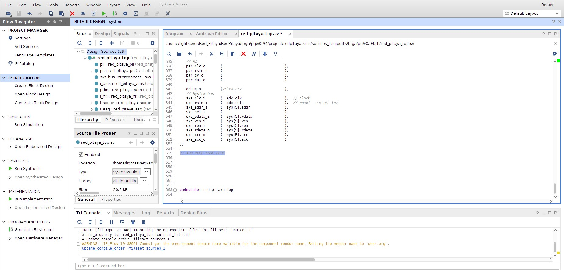
You can connect newly added sources in the Diagram (Block Design) section (If it is not open: Window => Design => double click system). Add them to the design by right click => Add Module in the design window (for more information check the Learn FPGA programming => FPGA lessons section) https://redpitaya-knowledge-base.readthedocs.io/en/latest/learn_fpga/4_lessons/top.html
Note
Before you try to Run Synthesis, Run Implementation, or Write Bitstream, you should check Language and Region settings on your Ubuntu/Linux computer – make sure you have a Format that uses a dot (“.”) as a decimal separator (the United Kingdom or the United States will work). Otherwise, the Synthesis might fail as some parts of Vivado demand a dot as the decimal separator, which will, in turn, cause Vivado not to recognize certain parts of the model.
The resulting .bit file is located in <Red Pitaya repository>/fpga/prj/<project name>/project/redpitaya.runs/impl_1/red_pitaya_top.bit This file must be copied to the Red Pitaya Linux OS into the /opt/redpitaya/fpga directory.
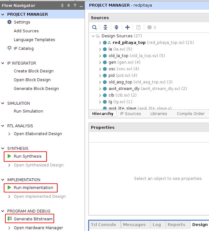
Run Synthesis
Run Implementation
Generate Bitstream
The resulting .bit file is located in <Red Pitaya repository>/fpga/prj/<project name>/project/redpitaya.runs/impl_1/ as red_pitaya_top.bit (the name of the .bit file is the same as the top module of the design).
3.2.2.3.4.1. Reprogramming the FPGA with a custom image
How the FPGA is reprogrammed depends on the OS version as well as whether the project has been executed in project mode (GUI) or non-project mode.
Please make sure that the PATH environment variable is set correctly. See Step 2 in the chapter above.
Note
On Windows, the process can also be done through a standard Command Prompt, but any echo commands must be executed inside the Windows Subsystem for Linux (WSL) Terminal (The output file encoding is a problem with Windows echo). For more information, refer to the following forum topics:
Please note that you need to change the forward slashes to backward slashes on Windows.
Open Terminal or CMD and go to the .bit file location.
cd <Path/to/RedPitaya/repository>/prj/v0.94/project/repitaya.runs/impl_1
Send the file .bit (red_pitaya_top.bit is the default name) to the Red Pitaya with the
scpcommand.scp red_pitaya_top.bit root@rp-xxxxxx.local:/root
Now establish an SSH communication with your Red Pitaya and check if you have the copy red_pitaya_top.bit in the root directory.
redpitaya> lsLoad the red_pitaya_top.bit to xdevcfg with
redpitaya> cat red_pitaya_top.bit > /dev/xdevcfg
The 2.00 OS uses a new mechanism of loading the FPGA. The process will depend on whether you are using Linux or Windows as the echo command functinality differs bewteen the two.
Please note that you need to change the forward slashes to backward slashes on Windows.
Non-project mode: Skip to step 3.
On Windows, open Vivado HSL Command Prompt and go to the .bit file location.
On Linux, open the Terminal and go to the .bit file location.
cd <Path/to/RedPitaya/repository>/prj/v0.94/project/repitaya.runs/impl_1
Create .bif file (for example, red_pitaya_top.bif) and use it to generate a binary bitstream file (red_pitaya_top.bit.bin)
Windows (Vivado HSL Command Prompt):
echo all:{ path/to/bitfile/fpga.bit } >  path/to/biffile/fpga.bif
bootgen -image path/to/biffile/fpga.bif -arch zynq -process_bitstream bin -o path/to/binfile/red_pitaya.bit.bin -w
Example code:
echo all:{ red_pitaya_top.bit } >  red_pitaya_top.bif
bootgen -image red_pitaya_top.bif -arch zynq -process_bitstream bin -o red_pitaya_top.bit.bin -w
Linux and Windows (WSL + Normal CMD):
echo -n "all:{ red_pitaya_top.bit }" >  red_pitaya_top.bif
bootgen -image red_pitaya_top.bif -arch zynq -process_bitstream bin -o red_pitaya_top.bit.bin -w
Send the file .bit.bin to the Red Pitaya with the
scpcommand.scp red_pitaya_top.bit.bin root@rp-xxxxxx.local:/root
Now establish an SSH communication with your Red Pitaya and check if you have the copy red_pitaya_top.bit.bin in the root directory.
redpitaya> lsLoad the red_pitaya_top.bit.bin image into the FPGA:
redpitaya> /opt/redpitaya/bin/fpgautil -b red_pitaya_top.bit.bin
3.2.2.3.4.2. Reverting to original FPGA image
If you want to roll back to the official Red Pitaya FPGA program, run the following command:
redpitaya> cat /opt/redpitaya/fpga/fpga_0.94.bit > /dev/xdevcfg
redpitaya> overlay.sh v0.94
or simply restart your Red Pitaya.
3.2.2.3.5. Programming via JTAG
These instructions show how to use a JTAG cable to program a Red Pitaya directly from Xilinx Vivado. To do so we use Red Pitaya STEMlab 125-14, Ubuntu 20.04, Vivado 2020.1, Digilent JTAG-HS3 cable with a 14 to 6-pin adapter, and Digilent Adept 2 software.
To start, get an appropriate JTAG cable. In these instructions, we use a Digilent JTAG-HS3 cable with a 14 to 6-pin adapter. Digilent JTAG-HS2 may be used as well and might be more appropriate, as it uses a 6-pin connector that can connect directly to Red Pitaya’s JTAG. For a complete list of JTAG cables, supported by Vivado, see Xilinx UG908 - Programming and Debugging, appendix D. https://www.xilinx.com/content/dam/xilinx/support/documentation/sw_manuals/xilinx2021_2/ug908-vivado-programming-debugging.pdf
See if the JTAG cable is detected. In Ubuntu, that is done with:
$ lsusb
JTAG-HS3 is displayed as an FTDI device.

Now, install Digilent Adept 2 software from https://digilent.com/reference/software/adept/start. You will need both Utilities and Runtime. These are both available as .deb packages. If installing from GUI does not work, they can be installed using:
$ sudo dpkg -i <path to package>
Once these packages are installed, you can check if the driver detects your adapter (only applies to Digilent cables):
$ djtgcfg enum

Now, open Vivado 2020.1, click Program and Debug -> Open Target -> Auto Connect.
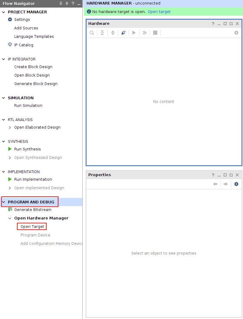
This will display a Xilinx-compatible JTAG cable in the Hardware window, under localhost.
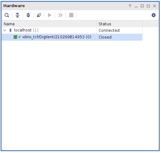
Now plug your cable into Red Pitaya’s JTAG connector. The pins are marked on the bottom side of Red Pitaya’s PCB.
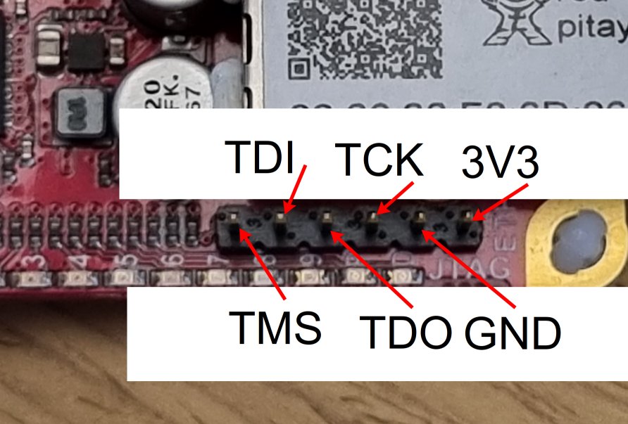
A Xilinx device should now appear in Vivado (on the detected cable). In this case, it’s an xc7z010_1.
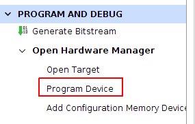
Now, you can click Program Device.
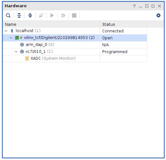
A bitfile selector prompt appears and when a valid file is selected, Red Pitaya can be programmed.
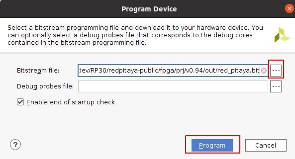
3.2.2.3.6. Simulation
ModelSim as provided for free from Altera is used to run simulations. Scripts expect the default install location. On Ubuntu, the install process fails to create an appropriate path to executable files, so this path must be created:
$ ln -s $HOME/intelFPGA/16.1/modelsim_ase/linux $HOME/intelFPGA/16.1/modelsim_ase/linux_rh60
$ sudo apt install libxft2:i386
To run the simulation, Vivado tools have to be installed.
There is no need to source settings.sh.
For now, the path to the ModelSim simulator is hard coded into the simulation Makefile.
$ cd fpga/sim
Simulations can be run by running make with the bench file name as target:
$ make top_tb
Some simulations have a waveform window configuration script like top_tb.tcl
which will prepare an organized waveform window.
$ make top_tb WAV=1
3.2.2.3.7. Device tree
The device tree is used by Linux to describe features and address the space of memory-mapped hardware attached to the CPU.
Running make of a project will create a device tree source and some include files in the directory dts:
device tree file |
contents |
|---|---|
zynq-7000.dtsi |
Description of peripherals inside PS (processing system) |
pl.dtsi |
description of AXI attached peripherals inside PL (programmable logic) |
system.dts |
description of all peripherals, includes the above |
To enable some Linux drivers (Ethernet, XADC, I2C EEPROM, SPI, GPIO, and LED) additional configuration files.
Generic device tree files can be found in fpga/dts while project-specific code is in fpga/prj/name/dts/.
3.2.2.3.8. Signal mapping
3.2.2.3.8.1. XADC inputs
XADC input data can be accessed through the Linux IIO (Industrial IO) driver interface.
E2 con |
schematic |
ZYNQ p/n |
XADC in |
IIO filename |
Measurement target |
Full scale range |
|---|---|---|---|---|---|---|
AI0 |
AIF[PN]0 |
B19/A20 |
AD8 |
in_voltage11_raw |
general purpose |
3.50 V |
AI1 |
AIF[PN]1 |
C20/B20 |
AD0 |
in_voltage9_raw |
general purpose |
3.50 V |
AI2 |
AIF[PN]2 |
E17/D18 |
AD1 |
in_voltage10_raw |
general purpose |
3.50 V |
AI3 |
AIF[PN]3 |
E18/E19 |
AD9 |
in_voltage12_raw |
general purpose |
3.50 V |
AIF[PN]4 |
K9 /L10 |
AD |
in_voltage8_vpvn_raw |
5V power supply |
6.10 V |
3.2.2.3.8.1.1. Input range
The default mounting intends for unipolar XADC inputs, which allow for observing only positive signals with a saturation range of 0 V ~ 0.5 V. There are additional voltage dividers use to extend this range to 0 V ~ 3.5 V.
It is possible to configure XADC inputs into a bipolar mode with a range of -0.5 V ~ +0.5 V, but it requires removing R273 and providing a 0.5 V ~ 1 V common voltage on the E2 connector. Please consult the schematics for more details.
3.2.2.3.8.1.1.1. 5V power supply
                       ------------------0  Vout
          -----------  |  -----------
Vin  0----| 56.0 kΩ |-----| 4.99 kΩ |----0  GND
          -----------     -----------
3.2.2.3.8.1.1.2. General purpose inputs
                       ------------------0  Vout
          -----------  |  -----------
Vin  0----| 30.0 kΩ |-----| 4.99 kΩ |----0  GND
          -----------     -----------
3.2.2.3.8.2. GPIO and LEDs
Handling of GPIO and LED signals depends on whether they are connected to Zynq-7000 PS (MIO) or PL (EMIO or FPGA) block.
MIO pins signals are controlled by the PS block. Each pin has a few multiplexed functions. The multiplexer, slew rate, and pull-up resistor enable can be controlled using software usually with device tree pinctrl code. Xilinx also provides Linux drivers for all PS based peripherals, so all MIO signals can be managed using Linux drivers.
Pins connected to the PL block require FPGA code to function. If the pin signals are wired directly (in the FPGA sources) from PS-based EMIO signals to the FPGA pads, then they can be managed using Linux drivers intended for the PS block.
The default pin assignment for GPIO is described in the next table.
FPGA |
Connector |
GPIO |
MIO/EMIO index |
|
Comments, LED color, dedicated meaning |
|---|---|---|---|---|---|
green, Power Good status |
|||||
blue, FPGA programming DONE |
|||||
|
|
|
|||
|
|
|
|||
LED |
|
|
yellow |
||
LED `` [8]`` |
|
|
yellow = SD card access (user defined) |
||
LED `` [9]`` |
|
|
red = CPU heartbeat (user defined) |
||
|
|
UART1_TX |
|
|
output only |
|
|
UART1_RX |
|
|
requires |
|
|
SPI1_MOSI |
|
|
requires |
|
|
SPI1_MISO |
|
|
requires |
|
|
SPI1_SCK |
|
|
requires |
|
|
SPI1_CS# |
|
|
requires |
|
|
I2C0_SCL |
|
|
requires |
|
|
I2C0_SDA |
|
|
requires |
3.2.2.3.8.3. Linux access to LED
This document is used as a reference: http://www.wiki.xilinx.com/Linux+GPIO+Driver
By providing GPIO/LED details in the device tree, it is possible to access LEDs using a dedicated kernel interface.
To show CPU load on LED 9 use:
$ echo heartbeat > /sys/class/leds/led0/trigger
To switch LED 8 ON use:
$ echo 1 > /sys/class/leds/led0/brightness
3.2.2.3.8.4. PS pinctrl for MIO signals
It is possible to modify MIO pin functionality using device tree files during Linux bootup. The listed files should be included in the main device tree.
These files can be modified into device tree overlays, which can be used to modify MIO functionality at runtime.
device tree file |
description |
|---|---|
|
E2 connector, SPI1 signals are repurposed as GPIO |
|
E2 connector, I2C0 signals are repurposed as GPIO |
|
E2 connector, UART1 signals are repurposed as GPIO |
|
E2 connector, SPI1 MISO signal is repurposed as GPIO SPI can then only be used for writing (maybe 3-wire) |