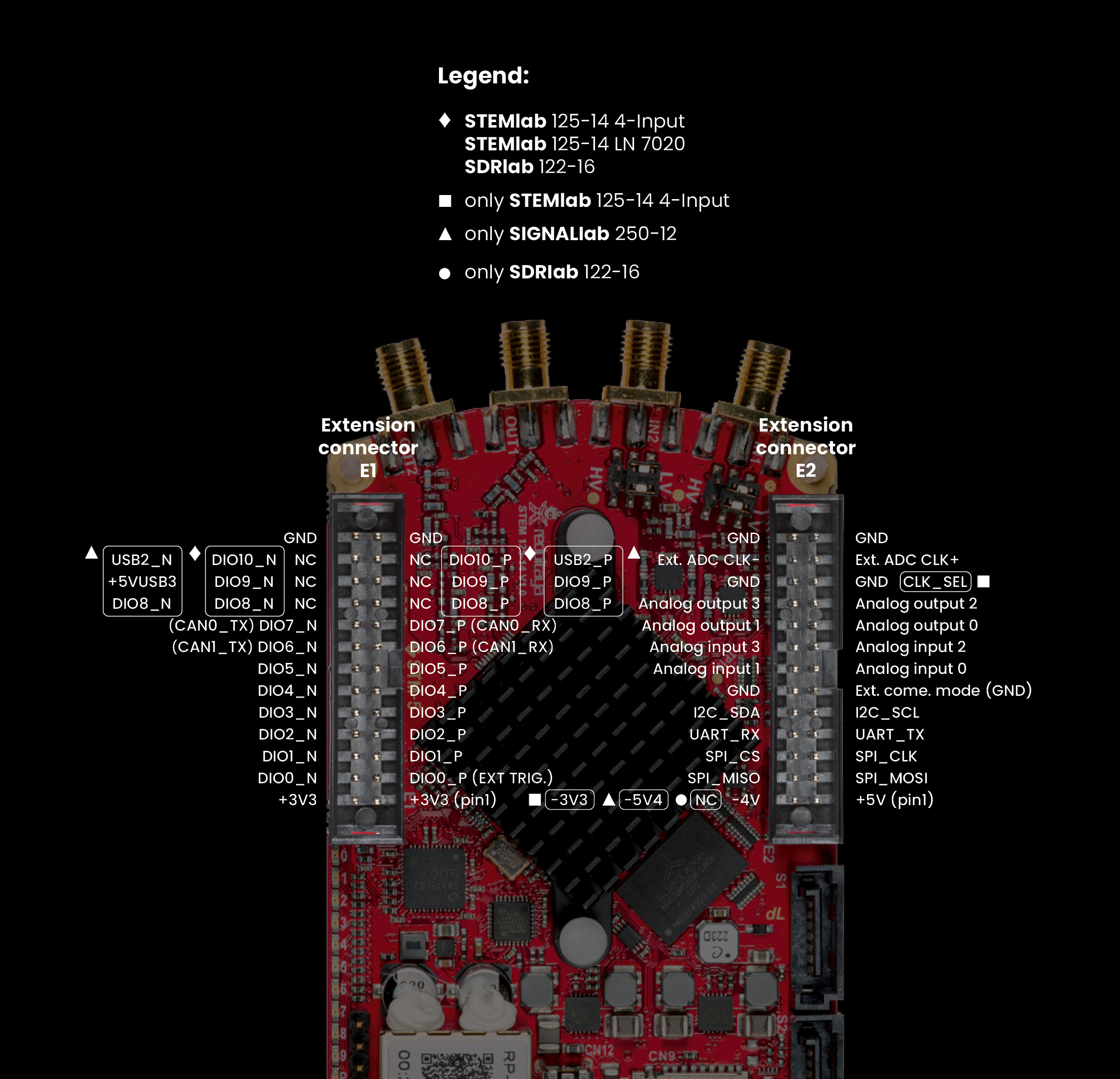
3.1.1.3. STEMlab 125-14 external clock
This STEMlab version is standard STEMlab 125-14 modified in such a way that the ADC and DAC clock can be provided from an external source clock. An external clock should be connected to the Ext ADC CLK- and + pins. According to the ADC spec, external clock signal levels should be LVDS in the range from 1 MHz to 125 MHz.
Note
The OS will not boot without providing an external clock.
3.1.1.3.1. Pinout
3.1.1.3.2. Technical specifications
Basic |
|
|---|---|
Processor |
DUAL CORE ARM CORTEX A9 |
FPGA |
FPGA Xilinx Zynq 7010 SOC |
RAM |
512 MB (4 Gb) |
System memory |
Micro SD up to 32 GB |
Console connection |
Micro USB |
Power connector |
Micro USB |
Power consumption |
5 V, 2 A max |
Connectivity |
|
|---|---|
Ethernet |
1 Gbit |
USB |
USB 2.0 |
Wi-Fi |
requires Wi-Fi dongle |
RF inputs |
|
|---|---|
RF input channels |
2 |
Sample rate |
125 MS/s |
ADC resolution |
14 bit |
Input impedance |
1 MΩ / 10 pF |
Full scale voltage range |
±1 V (LV) and ±20 V (HV) |
Input coupling |
DC |
Absolute max. Input voltage range |
30 V |
Input ESD protection |
Yes |
Overload protection |
Protection diodes |
Bandwidth |
DC - 60 MHz |
RF outputs |
|
|---|---|
RF output channels |
2 |
Sample rate |
125 MS/s |
DAC resolution |
14 bit |
Load impedance |
50 Ω |
Voltage range |
±1 V |
Short circuit protection |
Yes |
Connector type |
SMA |
Output slew rate |
2 V / 10 ns |
Bandwidth |
DC - 50 MHz |
Extension connector |
|
|---|---|
Digital IOs |
16 |
Analog inputs |
4 |
Analog inputs voltage range |
0-3.5 V |
Sample rate |
100 kS/s |
Resolution |
12 bit |
Analog outputs |
4 |
Analog outputs voltage range |
0-1.8 V |
Communication interfaces |
I2C, SPI, UART, CAN |
Available voltages |
+5 V, +3.3 V, -4 V |
External ADC clock |
Yes |
Synchronisation |
|
|---|---|
Trigger input |
Through extension connector |
Daisy chain connection |
Over SATA connection (up to 500 Mbps) |
Ref. clock input |
N/A |
Note
For more information, please refer to the Product comparison table.
3.1.1.3.2.1. Schematics
Note
FULL HW schematics for the Red Pitaya board are not available. Red Pitaya has open-source code but not open hardware schematics. Nonetheless, DEVELOPMENT schematics are available. This schematic will give you information about HW configuration, FPGA pin connections, and similar.
3.1.1.3.2.2. Mechanical Specifications and 3D Models
3.1.1.3.2.3. ADC specifications
3.1.1.3.2.4. Red Pitaya clock wiring
3.1.1.3.2.5. Other specifications
For all other specifications please refer to standard STEMlab 125-14 specs.
