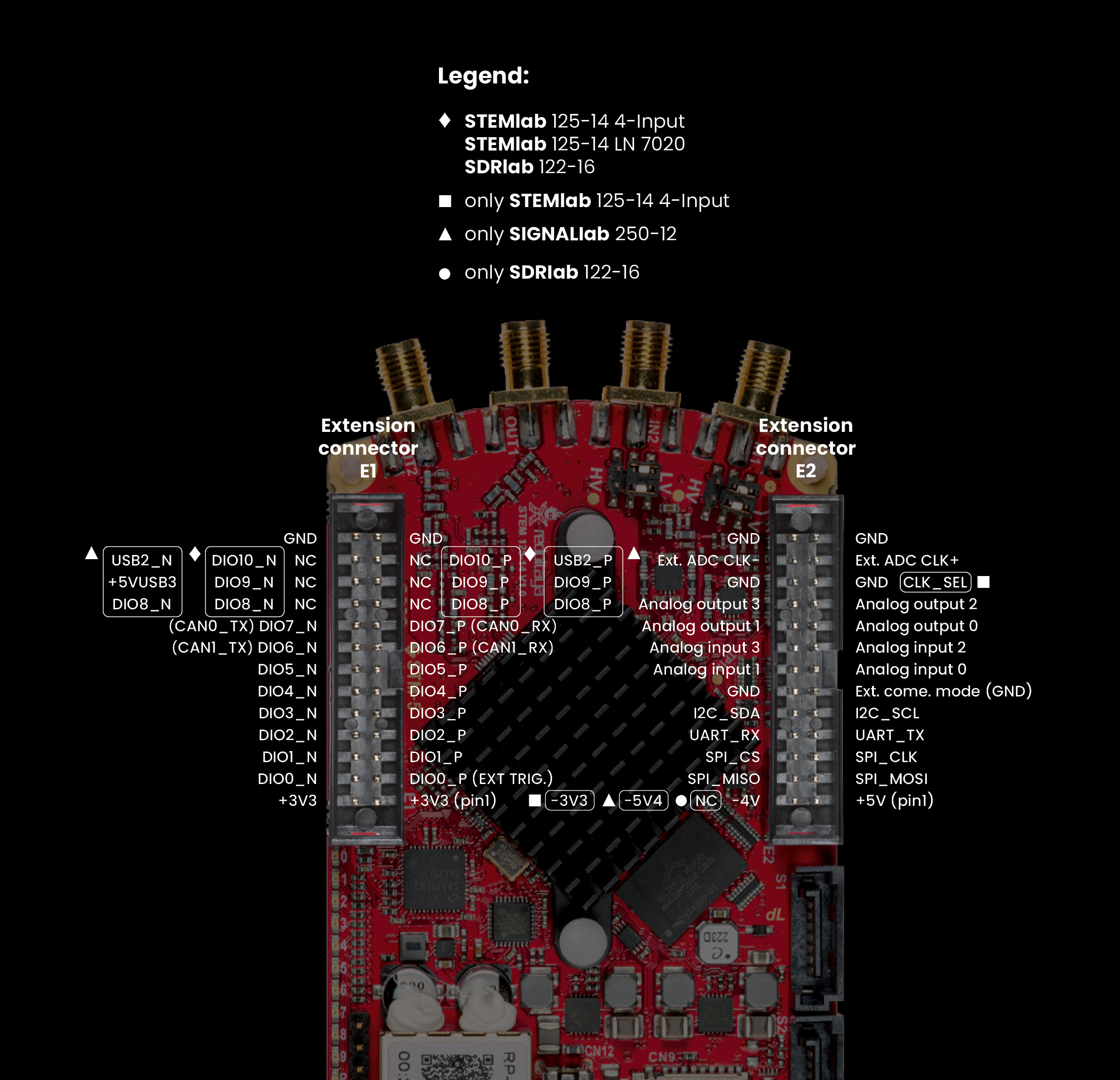
3.1.1.2.7.1. Extension connector
Connector: 2 x 26 pins IDC (M)
Power supply:
Available voltages: +5 V, +3.3 V, -3.4 V
Current limitations: 500 mA for +5 V and +3.3 V (to be shared between extension module and USB devices), 50 mA for -3.4 V supply.
3.1.1.2.7.1.1. Extension connector E1
3v3 power source
16 single ended or 8 differential digital I/Os with 3.3 V logic levels
Pin |
Description |
FPGA pin number |
FPGA pin description |
Voltage levels |
|---|---|---|---|---|
1 |
3V3 |
|||
2 |
3V3 |
|||
3 |
DIO0_P / EXT TRIG |
G17 |
IO_L16P_T2_35 |
3.3V |
4 |
DIO0_N |
G18 |
IO_L16N_T2_35 |
3.3V |
5 |
DIO1_P |
H16 |
IO_L13P_T2_MRCC_35 |
3.3V |
6 |
DIO1_N |
H17 |
IO_L13N_T2_MRCC_35 |
3.3V |
7 |
DIO2_P |
J18 |
IO_L14P_T2_AD4P_SRCC_35 |
3.3V |
8 |
DIO2_N |
H18 |
IO_L14N_T2_AD4N_SRCC_35 |
3.3V |
9 |
DIO3_P |
K17 |
IO_L12P_T1_MRCC_35 |
3.3V |
10 |
DIO3_N |
K18 |
IO_L12N_T1_MRCC_35 |
3.3V |
11 |
DIO4_P |
L14 |
IO_L22P_T3_AD7P_35 |
3.3V |
12 |
DIO4_N |
L15 |
IO_L22N_T3_AD7N_35 |
3.3V |
13 |
DIO5_P |
L16 |
IO_L11P_T1_SRCC_35 |
3.3V |
14 |
DIO5_N |
L17 |
IO_L11N_T1_SRCC_35 |
3.3V |
15 |
DIO6_P / CAN1_RX |
K16 |
IO_L24P_T3_AD15P_35 |
3.3V |
16 |
DIO6_N / CAN1_TX |
J16 |
IO_L24N_T3_AD15N_35 |
3.3V |
17 |
DIO7_P / CAN0_RX |
M14 |
IO_L23P_T3_35 |
3.3V |
18 |
DIO7_N / CAN0_TX |
M15 |
IO_L23N_T3_35 |
3.3V |
19 |
NC |
|||
20 |
NC |
|||
21 |
NC |
|||
22 |
NC |
|||
23 |
NC |
|||
24 |
NC |
|||
25 |
GND |
|||
26 |
GND |
Note
To switch the functionality of DIO6_P, DIO6_N, DIO7_P and DIO7_N from GPIO to CAN, please change the Housekeeping register value at address 0x34. For more information, please reffer to the FPGA register section (this feature is currently under development).
- All DIOx_y pins are LVCMOS33, with the following abs. max. ratings:
min. -0.40 V
max. 3.3 V + 0.55 V
<8 mA drive strength
3.1.1.2.7.1.2. Extension connector E2
+5 V & -3V4 power source
SPI, UART, I2C
4 x slow ADCs
4 x slow DACs
Ext. clock for fast ADC
Pin |
Description |
FPGA pin number |
FPGA pin description |
Voltage levels |
|---|---|---|---|---|
1 |
+5V |
|||
2 |
NC |
|||
3 |
SPI (MOSI) |
E9 |
PS_MIO10_500 |
3.3 V |
4 |
SPI (MISO) |
C6 |
PS_MIO11_500 |
3.3 V |
5 |
SPI (SCK) |
D9 |
PS_MIO12_500 |
3.3 V |
6 |
SPI (CS) |
E8 |
PS_MIO13_500 |
3.3 V |
7 |
UART (TX) |
D5 |
PS_MIO8_500 |
3.3 V |
8 |
UART (RX) |
B5 |
PS_MIO9_500 |
3.3 V |
9 |
I2C (SCL) |
B9 |
PS_MIO50_501 |
3.3 V |
10 |
I2C (SDA) |
B13 |
PS_MIO51_501 |
3.3 V |
11 |
Ext com.mode |
GND (default) |
||
12 |
GND |
|||
13 |
Analog Input 0 |
B19, A20 |
IO_L2P_T0_AD8P_35, IO_L2N_T0_AD8N_35 |
0-3.5 V |
14 |
Analog Input 1 |
C20, B20 |
IO_L1P_T0_AD0P_35, IO_L1N_T0_AD0N_35 |
0-3.5 V |
15 |
Analog Input 2 |
E17, D18 |
IO_L3P_T0_DQS_AD1P_35, IO_L3N_T0_DQS_AD1N_35 |
0-3.5 V |
16 |
Analog Input 3 |
E18, E19 |
IO_L5P_T0_AD9P_35, IO_L5N_T0_AD9N_35 |
0-3.5 V |
17 |
Analog Output 0 |
T10 |
IO_L1N_T0_34 |
0-1.8 V |
18 |
Analog Output 1 |
T11 |
IO_L1P_T0_34 |
0-1.8 V |
19 |
Analog Output 2 |
P15 |
IO_L24P_T3_34 |
0-1.8 V |
20 |
Analog Output 3 |
U13 |
IO_L3P_T0_DQS_PUDC_B_34 |
0-1.8 V |
21 |
GND |
|||
22 |
GND |
|||
23 |
Ext Adc CLK+ |
LVDS |
||
24 |
Ext Adc CLK- |
LVDS |
||
25 |
GND |
|||
26 |
GND |
1 Red Pitaya Version 1.0 has -3.3 V on pin 2. Red Pitaya Version 1.1 has -3.4 V on pin 2.
Schematics of extension connectors are shown in the picture below.
Notes:
Input capacitance depends on jumper settings and may vary.
A 50 Ω termination can be connected through an SMA tee in parallel to the input for measurements in a 50 Ω system.
Crosstalk measured with a high gain jumper setting on both channels. The SMA connectors not involved in the measurement are terminated.
Measurement referred to high gain jumper setting with limited environmental noise, inputs and outputs terminated, output signals disabled, and the PCB grounded through SMA ground. The specified noise floor measurement is calculated from the standard deviation of 16k contiguous samples at full rate. (Typically full bandwidth std(Vn) < 2 mV). The noise floor specification does not treat spurious spectral components separately and represents a time domain noise average referred to a 1 Hz bandwidth. In the presence of spurious components, the actual noise floor would be lower.
Measurement referred at high gain jumper setting, inputs matched and outputs terminated, outputs signal disabled, PCB grounded through SMA ground.
Measurement referred to high gain jumper setting, inputs and outputs terminated, outputs signal disabled, PCB grounded through SMA ground.
Further corrections can be applied through more precise gain and DC offset calibration.
Default software enables sampling at CPU dependent speed. The acquisition of sequence at 100 ksps rate requires the implementation of additional FPGA processing.
First order low pass filter implementation. Additional filtering can be externally applied according to application requirements.
The output channels are designed to drive 50 Ω loads. Terminate outputs when channels are not used. Connect parallel 50 Ω load (SMA tee junction) in high impedance load applications.
Measured at 10 dBm output power level
The typical power level with 1 MHz sine is 9.5 dBm. Output power is subject to slew rate limitations.
The detailed scheme can be found in the documentation (Red_Pitaya_Schematics_v1.0.1.pdf).
To avoid speed limitations on digital General Purpose Input / Output pins are directly connected to the FPGA. FPGA decoupling and pin protection is to be addressed within extension module designs. The user is responsible for pin handling.
The use of an unapproved power supply may deteriorate performance or damage the product.
A heatsink must be installed and the board must be operated on a flat surface without airflow obstructions. Operation at higher ambient temperatures and lower pressure conditions within enclosures will be addressed by means of adequate ventilation. The operation of the product is automatically disabled at increased temperatures.
Some parts may become hot during and after operation. Do not touch them.
Measurement performance is specified within this range.
Valid for low frequency signals. For input signals that contain frequency components beyond 1 kHz, the full scale value defines the maximum admissible input voltage.
The jumper settings are limited to the positions described in the user manual. Any other configuration or use of different jumper types may damage the product and void the warranty.
The SMA connectors on the cables connected to Red Pitaya must correspond to the standard MILC39012. It’s important that the central pin is of a suitable length, otherwise the SMA connector installed on the Red Pitaya will mechanically damage the SMA connector. The central pin of the SMA connector on Red Pitaya will lose contact with the board and the board will not be possible to repair due to the mechanical damage (separation of the pad from the board).
Jumpers are not symmetrical; they have latches. Always install jumpers with the latch on its outer side in order to avoid problems with hard to remove jumpers.
Dimensions are rounded to the nearest millimeter. For exact dimensions, please see the technical drawings and product model. (Red_Pitaya_Dimensions_v1.0.1.pdf)
Information furnished by Red Pitaya d.o.o. is believed to be accurate and reliable. However, no responsibility is assumed for its use. Contents may be subject to change without any notice.
3.1.1.2.7.1.3. Auxiliary analog input channels
Number of channels: 4
Nominal sampling rate: 100 ksps (H)
ADC resolution 12 bits
Connector: dedicated pins on IDC connector E2 (pins 13,14,15,16)
Input voltage range: 0 to +3.5 V
Input coupling: DC
3.1.1.2.7.1.4. Auxiliary analog output channels
Number of channels: 4
Output type: Low pass filtered PWM (I)
PWM time resolution: 4 ns (1/250 MHz)
Connector: dedicated pins on IDC connector E2 (pins 17,18,19,20) v - Output voltage range: 0 to +1.8 V
Output coupling: DC
3.1.1.2.7.1.5. General purpose digital input/output channels: (N)
Number of digital input/output pins: 16
Voltage level: 3.3 V
Direction: configurable
Location: IDC connector E1 (pins 324)
3.1.1.2.7.1.6. Powering Red Pitaya through extension connector
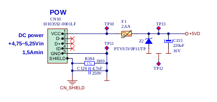
The Red Pitaya can also be powered through pin 1 of the extension connector E2, but in such a case, external protection must be provided by the user in order to protect the board!

Protection circuit between +5 V that is provided over the micro USB power connector and +5 VD that is connected to pin1 of the extension connector E2.
