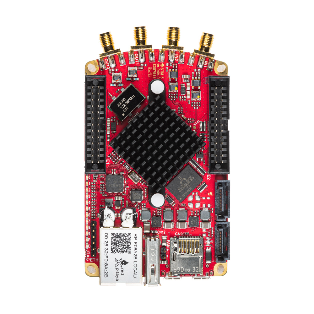
3.1.1.8. SDRlab 122-16
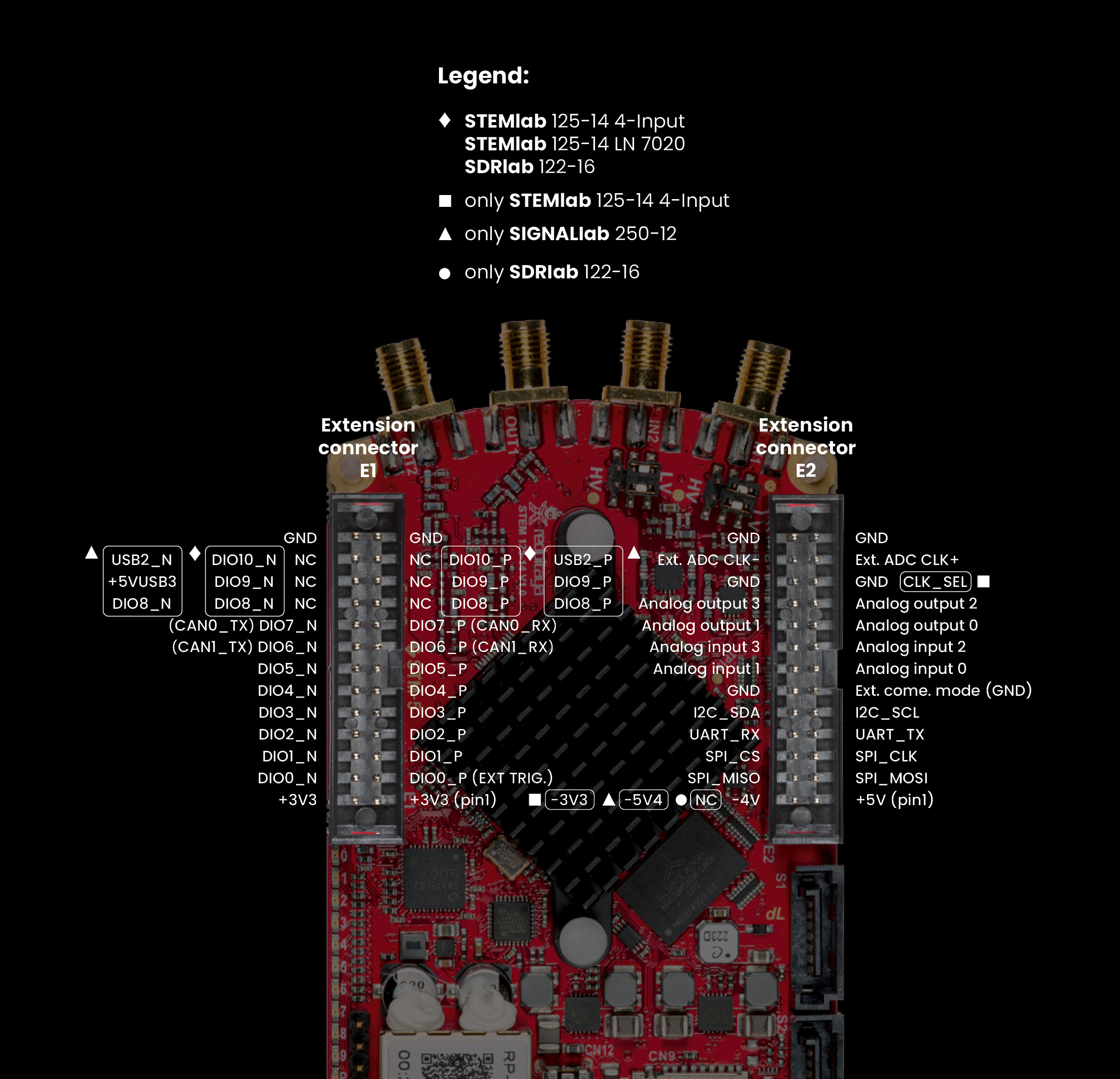
3.1.1.8.1. Pinout
3.1.1.8.2. Technical specifications
Basic |
|
|---|---|
Processor |
DUAL CORE ARM CORTEX A9 |
FPGA |
FPGA Xilinx Zynq 7020 SOC |
RAM |
512 MB (4 Gb) |
System memory |
Micro SD up to 32 GB |
Console connection |
Micro USB |
Power connector |
Micro USB |
Power consumption |
5 V, 2 A max |
Connectivity |
|
|---|---|
Ethernet |
1 Gbit |
USB |
USB 2.0 |
Wi-Fi |
requires Wi-Fi dongle |
RF inputs |
|
|---|---|
RF input channels |
2 |
Sample rate |
122.88 MS/s |
ADC resolution |
16 bit |
Input impedance |
50 Ω |
Full scale voltage range |
0.5 Vpp/-2 dBm |
Input coupling |
AC |
Absolute max. Input voltage range |
DC max 50 V (AC-coupled),
1 Vpp for RF
|
Input ESD protection |
Yes |
Overload protection |
DC voltage protection |
Bandwidth |
300 kHz - 550 MHz (undersampling) |
RF outputs |
|
|---|---|
RF output channels |
2 |
Sample rate |
122.88 MS/s |
DAC resolution |
14 bit |
Load impedance |
50 Ω |
Voltage range |
0.5 Vpp/-2 dBm (50 Ω load) |
Short circuit protection |
N/A, RF transformer & AC-coupled |
Connector type |
SMA |
Output slew rate |
N/A |
Bandwidth |
300 kHz - 60 MHz |
Extension connector |
|
|---|---|
Digital IOs |
22 |
Analog inputs |
4 |
Analog inputs voltage range |
0-3.5 V |
Sample rate |
100 kS/s |
Resolution |
12 bit |
Analog outputs |
4 |
Analog outputs voltage range |
0-1.8 V |
Communication interfaces |
I2C, SPI, UART, CAN |
Available voltages |
+5 V, +3.3 V, -4 V |
External ADC clock |
Yes |
Synchronisation |
|
|---|---|
Trigger input |
Through extension connector |
Daisy chain connection |
Over SATA connection (up to 500 Mbps) |
Ref. clock input |
N/A |
Note
For more information, please refer to the Product comparison table.
3.1.1.8.3. Schematics
Note
Red Pitaya board HW FULL schematics are not available. Red Pitaya has an open-source code but not open hardware schematics. Nonetheless, DEVELOPMENT schematics are available. This schematic will give you information about HW configuration, FPGA pin connection and similar.
3.1.1.8.4. Mechanical Specifications and 3D Models
3.1.1.8.5. Components
QSPI (NOT POPULATED - see QSPI section for more information).
3.1.1.8.6. Extension connector SDRlab
Connector: 2 x 26 pins IDC (M)
- Power supply:
Available voltages: +5 V, +3.3 V
Current limitations: 500 mA for +5 V and +3.3 V (to be shared between extension module and USB devices)
3.1.1.8.6.1. Extension connector E1
3V3 power source
22 single ended or 8 differential digital I/Os with 3.3 V logic levels
Pin |
Description |
FPGA pin number |
FPGA pin description |
Voltage levels |
|---|---|---|---|---|
1 |
3V3 |
|||
2 |
3V3 |
|||
3 |
DIO0_P / EXT TRIG |
G17 |
IO_L16P_T2_35 |
3.3V |
4 |
DIO0_N |
G18 |
IO_L16N_T2_35 |
3.3V |
5 |
DIO1_P |
H16 |
IO_L13P_T2_MRCC_35 |
3.3V |
6 |
DIO1_N |
H17 |
IO_L13N_T2_MRCC_35 |
3.3V |
7 |
DIO2_P |
J18 |
IO_L14P_T2_AD4P_SRCC_35 |
3.3V |
8 |
DIO2_N |
H18 |
IO_L14N_T2_AD4N_SRCC_35 |
3.3V |
9 |
DIO3_P |
K17 |
IO_L12P_T1_MRCC_35 |
3.3V |
10 |
DIO3_N |
K18 |
IO_L12N_T1_MRCC_35 |
3.3V |
11 |
DIO4_P |
L14 |
IO_L22P_T3_AD7P_35 |
3.3V |
12 |
DIO4_N |
L15 |
IO_L22N_T3_AD7N_35 |
3.3V |
13 |
DIO5_P |
L16 |
IO_L11P_T1_SRCC_35 |
3.3V |
14 |
DIO5_N |
L17 |
IO_L11N_T1_SRCC_35 |
3.3V |
15 |
DIO6_P / CAN1_RX |
K16 |
IO_L24P_T3_AD15P_35 |
3.3V |
16 |
DIO6_N / CAN1_TX |
J16 |
IO_L24N_T3_AD15N_35 |
3.3V |
17 |
DIO7_P / CAN0_RX |
M14 |
IO_L23P_T3_35 |
3.3V |
18 |
DIO7_N / CAN0_TX |
M15 |
IO_L23N_T3_35 |
3.3V |
19 |
DIO8_P |
Y9 |
IO_L14P_T2_SRCC_13 |
3.3V |
20 |
DIO8_N |
Y8 |
IO_L14N_T2_SRCC_13 |
3.3V |
21 |
DIO9_P |
Y12 |
IO_L20P_T3_13 |
3.3V |
22 |
DIO9_N |
Y13 |
IO_L20N_T3_13 |
3.3V |
23 |
DIO10_P |
Y7 |
IO_L13P_T2_MRCC_13 |
3.3V |
24 |
DIO10_N |
Y6 |
IO_L13N_T2_MRCC_13 |
3.3V |
25 |
GND |
|||
26 |
GND |
Note
To switch the functionality of DIO6_P, DIO6_N, DIO7_P and DIO7_N from GPIO to CAN, please change the Housekeeping register value at address 0x34. For more information, please reffer to the FPGA register section (this feature is currently under development).
- All DIOx_y pins are LVCMOS33, with the following abs. max. ratings:
min. -0.40 V
max. 3.3 V + 0.55 V
<8 mA drive strength
3.1.1.8.6.2. Extension connector E2
+5 V power source
SPI, UART, I2C
4 x slow ADCs
4 x slow DACs
Ext. clock for fast ADC
Pin |
Description |
FPGA pin number |
FPGA pin description |
Voltage levels |
|---|---|---|---|---|
1 |
+5V |
|||
2 |
-4V2 |
|||
3 |
SPI (MOSI) |
E9 |
PS_MIO10_500 |
3.3 V |
4 |
SPI (MISO) |
C6 |
PS_MIO11_500 |
3.3 V |
5 |
SPI (SCK) |
D9 |
PS_MIO12_500 |
3.3 V |
6 |
SPI (CS) |
E8 |
PS_MIO13_500 |
3.3 V |
7 |
UART (TX) |
D5 |
PS_MIO8_500 |
3.3 V |
8 |
UART (RX) |
B5 |
PS_MIO9_500 |
3.3 V |
9 |
I2C (SCL) |
B9 |
PS_MIO50_501 |
3.3 V |
10 |
I2C (SDA) |
B13 |
PS_MIO51_501 |
3.3 V |
11 |
Ext com.mode |
GND (default) |
||
12 |
GND |
|||
13 |
Analog Input 0 |
B19, A20 |
IO_L2P_T0_AD8P_35, IO_L2N_T0_AD8N_35 |
0-3.5 V |
14 |
Analog Input 1 |
C20, B20 |
IO_L1P_T0_AD0P_35, IO_L1N_T0_AD0N_35 |
0-3.5 V |
15 |
Analog Input 2 |
E17, D18 |
IO_L3P_T0_DQS_AD1P_35, IO_L3N_T0_DQS_AD1N_35 |
0-3.5 V |
16 |
Analog Input 3 |
E18, E19 |
IO_L5P_T0_AD9P_35, IO_L5N_T0_AD9N_35 |
0-3.5 V |
17 |
Analog Output 0 |
T10 |
IO_L1N_T0_34 |
0-1.8 V |
18 |
Analog Output 1 |
T11 |
IO_L1P_T0_34 |
0-1.8 V |
19 |
Analog Output 2 |
P15 |
IO_L24P_T3_34 |
0-1.8 V |
20 |
Analog Output 3 |
U13 |
IO_L3P_T0_DQS_PUDC_B_34 |
0-1.8 V |
21 |
GND |
|||
22 |
GND |
|||
23 |
Ext Adc CLK+ |
LVDS |
||
24 |
Ext Adc CLK- |
LVDS |
||
25 |
GND |
|||
26 |
GND |
Note
UART TX (PS_MIO08) is output only and must be low level at power-up (no external pull-ups)!
3.1.1.8.7. External ADC clock
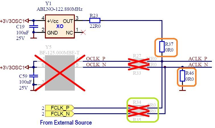
ADC clock can be provided by:
On board 122.88 MHz XO (default)
From external source / through extension connector (instructions provided below)
Warning
We do not advise altering the board because users have reported problems after doing so. Every board made has undergone rigorous testing, which cannot be claimed for modified boards. Any non-Red Pitaya hardware modification will void the warranty, and we cannot guarantee support for modified boards.
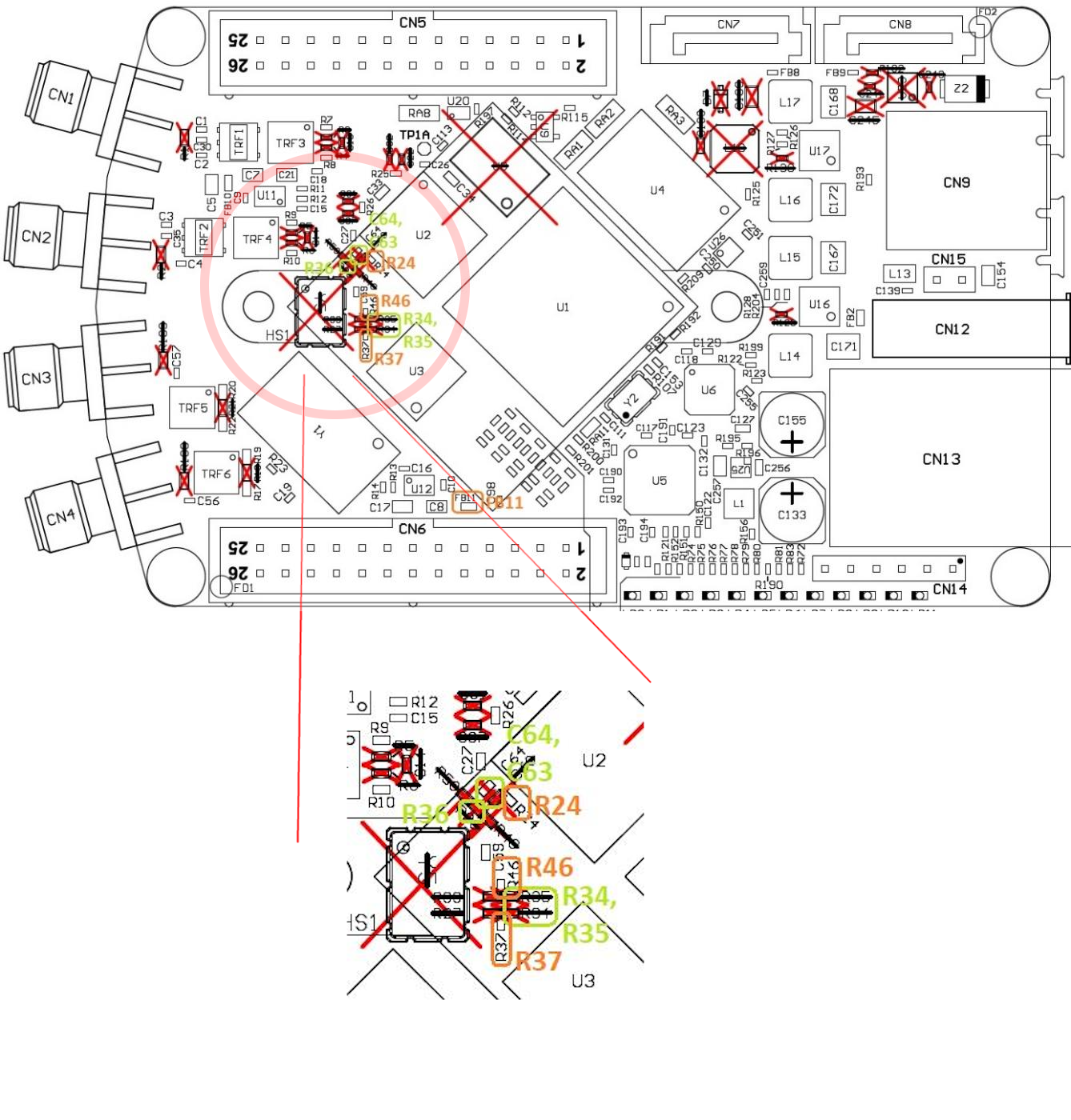
Remove: R37, R46
Add: R34 = 0R, R35 = 0R
Remove: FB11
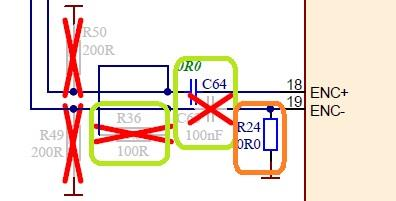
Remove: 0R on C64, R24
Add: C64 = 100nF, C63 = 100nF, R36 = 100R
3.1.1.8.8. Other specifications
For all other specifications please refer to standard STEMlab 125-14 specs.
Please note that the measurements on inputs will differ from the standard STEMlab 125-14.
